Experiment 11 - Exploring ATmega328 Peripherals
In this experiment, we explore ATmega328's built-in peripherals. Each experiment uses a selected peripheral in a specific application that demonstrates its functionality. Follow the procedure in Experiment 8 (see here) for setting up an ATMEL Studio project called "Experiment_11". Use the "main.asm" file here.
Note: The ZOC terminal is used in some of the example circuits.
Digital Input/Output Capability with the ATmega328
In Experiment 9 we configured and used 8-bit PORTS B, C, and D for digital I/O. In this experiment, we will use again digital I/O to output to LEDs with the added capability to input from a push button.
Before proceeding, let's utilize the assembler directive ".equ" to label the pins of the Redboard and associate them with the bit number of their respective digital I/O port. Once this is done, we can refer to them more conveniently by name rather than number. See the assembler directive code below.
;
; Pin Assignments
;
.equ pin0 = 0 ;Port d Bit 0
.equ pin1 = 1 ;Port d Bit 1
.equ pin2 = 2 ;Port d Bit 2
.equ pin3 = 3 ;Port d Bit 3
.equ pin4 = 4 ;Port d Bit 4
.equ pin5 = 5 ;Port d Bit 5
.equ pin6 = 6 ;Port d Bit 6
.equ pin7 = 7 ;Port d Bit 7
.equ pin8 = 0 ;Port b Bit 0
.equ pin9 = 1 ;Port b Bit 1
.equ pin10 = 2 ;Port b Bit 2
.equ pin11 = 3 ;Port b Bit 3
.equ pin12 = 4 ;Port b Bit 4
.equ pin13 = 5 ;Port b Bit 5
.equ pina0 = 0 ;Port c Bit 0
.equ pina1 = 1 ;Port c Bit 1
.equ pina2 = 2 ;Port c Bit 2
.equ pina3 = 3 ;Port c Bit 3
.equ pina4 = 4 ;Port c Bit 4
.equ pina5 = 5 ;Port c Bit 5
In addition, let's label the LEDs and Button so they will be easier to locate in our code.
;
; Define LED/Button Labels
;
.equ red_pin = pin9
.equ green_pin = pin10
.equ blue_pin = pin11
.equ button_1 = pin2
Note: ATmega328 documentation recommends that unless configured otherwise, all digital I/O should be configured as input with pull-up resistors enabled.
Following ATMEL's recommendation, we next configure all digital I/O ports to "input" with pull-up resistors enabled. In specific examples, we may reassign ports as needed.
;
; Digital I/O Initialization Code
;
clr r16
out ddrb,r16
;set all ports to input
out ddrc,r16
out ddrd,r16
ldi
r16,0xff ;enable all pull-up
resistors
out portb,r16
out portc,r16
out portd,r16
Try it!
Example Circuit 1 - Blinking a single red LED.
Connect the flat (-) lead of a red LED to ground through a 330 ohm resistor. Connect the rounded (+) lead to pin 9 of the Redboard.
For a microprocessor, blinking an LED is like the traditional "Hello World" that programmers use when exploring a new computer language.
The "set bit" instruction "sbi" highlighted in yellow below, modifies the initial configuration for PORT B pin 9 to output to drive the red LED connected to this pin.
Note: Using the set bit instruction, only the bit designated is changed; no other I/O register bits are affected.
We use the set bit "sbi" and clear bit "cbi" instructions to turn the red LED on and off with a one second delay. See the code highlighted in green.
;
; Example Circuit 1 - Blinking an LED (Digital I/O)
;
circuit_1:
;
; Setup Digital I/O
;
sbi
ddrb, red_pin ;set red LED
as output (port b bit 1)
;
; Main Program
;
circuit_1_again:
;
sbi
portb,red_pin ;turn on red
LED
call delay_1s
;delay 1 second
cbi
portb,red_pin ;turn off red LED
call delay_1s
;delay 1 second
rjmp circuit_1_again
;do again
;
Change the Target Jump line to "circuit_1". Connect a red LED from pin 9 through a 330 ohm resistor to ground. Build the solution and program the ATmega328 flash memory to test the program.
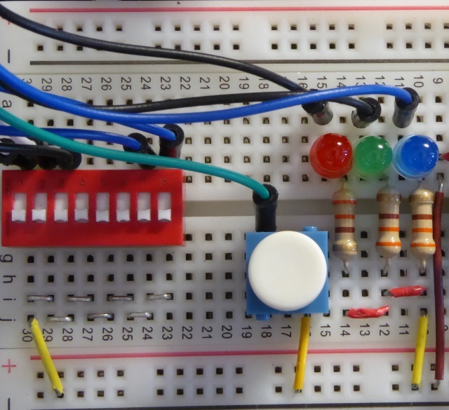
Example Circuit 2 - Rotate through a red, green, and blue LED whenever a button is pressed. The program begins with the red LED lighted. When the button is pressed the red LED extinguishes and the green LED lights. After additional pressings, the blue LED lights and then back to red before repeating.
Connect a green and blue LED as was done with the red LED above. The positive leads of the green and blue LEDs connect to pins 10 and 11 respectively. Install the normally open, push button switch (included with SparkFun Inventors Kit) with one lead connected to pin 2 (PORT D bit 2) and the other lead to ground. See the picture below.
The code below highlighted in yellow uses "sbi" and "cbi" instructions to set and clear I/O register bits associated with pins to which the three LEDs are connected. The code highlighted in orange configures the push button pin as input with pull-up resistor enabled.
The main program takes advantage of the fact that the three LEDs are connected to consecutive bits 1, 2, and 3 of PORT B. To start, 0b00000010 in R16 is output to PORT B lighting the red LED and turning off the green and blue. The DO-WHILE LOOP simply rotates R16 to the left so that the one bit moves successively to bit position 2 and 3 before starting over when a one in bit 4 is detected (highlighted in green). Outputting R16 after each rotation lights the LEDs in succession. The rotation waits at the point highlighted in blue by a call to the button debounce subroutine.
;
; Example Circuit 2 - Rotate through LEDs with button (Digital I/O)
;
circuit_2:
;
; Set Up Digital I/O
;
sbi
ddrb,red_pin
;set pin 9 Red LED as output (port b bit 1)
sbi
ddrb,green_pin
;set pin 10 Green LED as output (port b bit 2)
sbi
ddrb,blue_pin
;set pin 11 Blue LED as output (port b bit 3)
cbi
ddrd,button_1
;set pin 2 Button as input (port d bit 2)
sbi
portd,button_1
;enable pull-up resisitor on pin 2 Button 1 (port d bit 2)
;
; Main Program
;
circuit_2_again:
ldi zl,(1<<red_pin)
;start with red LED
circuit_2_loop:
out
portb,zl
;turn off previous LED and turn on next LED
call debounce_wait
;wait for button press and release
lsl
zl
sbrs
zl,(blue_pin+1)
;reached bit left of blue_pin?
rjmp
circuit_2_loop
;if not, display next LED
rjmp
circuit_2_again
;otherwise, start over
The button switch, like all mechanical switches, is inherently noisy. When the button is pressed, the contacts bounce several times before settling down to a stable state (either open or closed). Without debouncing, the LEDs in our program would change rapidly from one to the next as the switch contacts bounce. Comment out the call to the debounce subroutine and see the problem.
The debounce subroutine waits for a stable "switch is pressed" followed by a stable "switch is released" before returning to change to the next LED. While there are several ways to debounce switches, we chose a very clever one that works quite well. R16 is setup as a shift register initially filled with all ones. R17 is used to control whether we are looking for an all zeros in the shift register (button pressed - switch closed) or all ones (button released - switch open). Upon entering the subroutine, R17 is all zeros, so we are looking for all zeros in R16. The status of the switch (either one if open or zero if closed) is applied to the carry bit in the status register and then rotated into R16. This sequence is repeated at 5 ms intervals until eight consecutive zero rotations signal a stable "switch pressed". R17 is then set to all ones and the process repeated waiting for eight consecutive one rotations indicating a stable "switch released". At this, we return allowing the LEDs to rotate to the next color.
;
; Debounce
;
; Wait for button to be pressed then released before returning
;
; Input: None
;
; Returns: Nothing
;
; Registers Used: r16,r17,r18,x,y,sreg
;
debounce_wait:
;
ser
r16
;0xff -> r16
clr
r17
;setup to wait for all zeros first time
;
debounce_wait_loop:
;
ldiw xh,xl,5
;delay 5 milliseconds
call
delay_ms
in
r18,pind
;check button 1
clc
;pre-clear carry
sbrc
r18,button_1
;if button pressed, skip setting carry
sec
;if button not pressed, set carry
rol
r16
;rotate carry to r16 bit0
cp
r16,r17
;wait until r16 filled with all zeros first time or all ones second time
brne debounce_wait_loop
or
r17,r17
;if first time, setup to wait for all ones second time
ser r17
breq debounce_wait_loop
;after second time, return done
ret
Change the Target Jump line to "circuit_2". Build the solution and program the ATmega328 flash memory to test the program.
Analog-to-Digital Conversion with the ATmega328
Another useful ATmega328 peripheral is the analog-to-digital converter or simply "A/D converter". Six A/D channels are alternate functions of PORT C and are labeled on the Redboard as A0 to A5.
Try it!
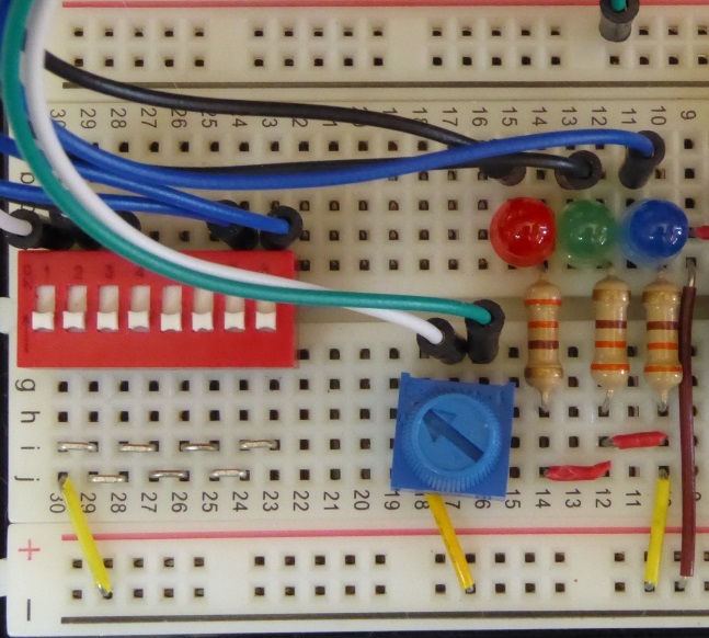
Example Circuit 3 - Vary the speed of the rotation for three LEDs with a potentiometer.
In this example, a potentiometer is connected as a voltage divider between Vcc (nominally 5 volts) and ground. Remove the push button switch and replace it with the potentiometer included with SparkFun Inventors Kit. Connect the right outside lead to Vcc and the left outside lead to ground. Connect the center lead (the wiper) to Redboard pin A0. By connecting the potentiometers wiper to A0, we provide an adjustable voltage of Vcc to 0 to the ATmega328's A/D channel 0. With this arrangement, the 10-bit A/D channel's digital value will range from 1023 to 0 as the potentiometer is rotated clockwise. This digital value is passed in register x to the "delay_ms" utility subroutine producing a potentiometer controlled delay between rotating LEDs. The breadboard configuration for Circuit Example 3 is pictured below.
Examining the program below, it is essentially the same as Circuit Example 2 with the push button removed and variable time delay code added.
Refer to section 28 of the ATmega328 Datasheet for a complete description of A/D operation.
To set up the A/D, we configure the ADMUX I/O register with a byte made up of four parts (see section 28.9.1):
(1) Bits 7-6 select the reference source. "01" selects Vcc, See Table 24-3.
(2) Bit 5 "0" selects no left adjust of the result. With this option, the most significant two bits in the converted value will be in bits 1 and 0 of I/O register ADCH with the remaining eight bits in ADCL.
(3) Bit 4 is always "0".
(4) Bits 3-0 selects the A/D channel "0000" is A/D 0 (pina0). For other A/D channels, see Table 24-4.
The assembled byte is written to I/O register ADMUX. Refer to the code highlighted in yellow below. The A/D converter is now ready to enable and start a conversion.
To start a conversion, we enable the A/D by setting bit ADEN bit 7; set the start conversion bit ADSC bit 6; and, using table 28-5, choose prescaler ADPS entry 128 by setting bits 2 to 0 in I/O register ADCSRA. See the code highlighted in green. The AA/D converter must be clocked between 50 Khz and 200 KHz. Given that the system clock is 16 MHz; a prescaler value of 128 gives an A/D clock of 125 Khz. Refer to section 28.9.2 for more details.
Execution then enters a WAIT-DO LOOP looking for ADSC (A/D start bit 6-the bit we set previously) to clear indicating conversion has completed. See the code highlighted in orange.
Lastly, the conversion result is loaded into the x register pair (I/O register ADCL into xl and I/O register ADCH into xh as shown in blue) and then passed to the "delay_ms" subroutine to provide a potentiometer controlled delay before the next LED lights.
Note: When reading 16-bit I/O register values as in this case, we must read the high byte first then the low byte. Writing to 16-bit I/O registers is reversed: Write to the high byte first then the low byte. See section 20.6 of the ATmega328 Data Sheet.
;
; Experiment Redboard 3 - Rotate through LEDs with with potentiometer based
delay (Analog Input)
;
circuit_3:
;
; Set Up Digital I/O
;
sbi ddrb,pin9
;set pin 9 Red LED as output (port b bit 1)
sbi
ddrb,pin10
;set pin 10 Green LED as output (port b bit 2)
sbi
ddrb,pin11
;set pin 11 Blue LED as output (port b bit 3)
;
; Set Up Analog-to-Digital Converter See Section 28.9.1
;
ldi
r16,0b01000000
;0bxxy0zzzz xx = 01 use internal AVcc for reference (See Table 28-3)
; y = 0 right adjust result (Search "Bit 5 – ADLAR")
; zzzz = 0000 A/D channel 0 (See Table 28-4)
sts
admux,r16
;ADC Multiplexer Selection Register
;
; Main Program
;
circuit_3_again:
;
ldi zl,(1<<red_pin)
;start with red LED
;
circuit_3_loop:
;
out portb,zl
;turn off previous LED and turn on next LED
;
; Start A/D Conversion See Section 28.9.1
;
ldi
r16,0b11000111 ;0bxy000zzz x = 1 enable A/D (Search "Bit 7 – ADEN")
; y = 1 start conversion (Search "Bit 6 – ADSC")
; zzz = 111 prescale = 128 (See "Table 28-5")
sts
adcsra,r16
;ADC Control and Status Register A
;
;
circuit_3_wait:
;
lds
r16,adcsra
;check if a/d conversion complete?
sbrc
r16,adsc
;adsc cleared?
rjmp
circuit_3_wait ;if not, wait
lds
xl,adcl
;a/d result in x
lds
xh,adch
call delay_ms
;delay x milliseconds
lsl
zl
sbrs zl,(blue_pin+1)
;reached bit left of blue_pin?
rjmp circuit_3_loop
;if not, display next LED
rjmp
circuit_3_again ;otherwise, start over
Change the Target Jump line to "circuit_3". Build the solution and program the ATmega328 flash memory to test the program.
Using an Alternate Way to Represent I/O Register Code
This is a good time to introduce an alternate way of representing I/O register code. Consider the part of the green code above that sets up the A/D register ADCSRA.
ldi
r16,0b11000111 ;0bxy000zzz x = 1 enable A/D (search "Bit 7 – ADEN")
; y = 1 start conversion (search "Bit 6 – ADSC")
; zzz = 111 prescale = 128 (search "Table 28-5")
From Section 28.9.2 we find the following labels and actual values for the components we need:
ADEN - A/D Enable = 1 (value = 7)
ADSC - Start conversion = 1 (value = 6)
ADPSn - A/D prescale where n = 0,1,2 (values = 0, 1, 2 respectively) in Table
28-5
Recall that the assembler interprets the expression 1<<n as 0b00000001 shifted left n times. Also, the vertical bar "|" character is interpreted as a bit-wise OR. Combining these elements we can build the AMCSRA option as shown below:
0b1100111 = 1<<ADEN | 1<<ADSC | 1<<ADPS2 | 1<<ADPS1 | 1<<ADPS0
In the expression, 1<<ADEN is actually 1<<7 or 0b00000001 shifted left 7 times giving 0b10000000. The remaining terms are similarly calculated and all are ORed together to give the final result 0b11000111. Labels (defined bits) not included in the expression resolve to zero. This approach may seem a little mysterious at first, but many assembly and C++ programmers use it. We will continue describing I/O register code explicitly as in the comments above, but it good to know the alternative.
Using the ATmega328 Counter/Timers
The ATmega328 has three counter/timers: two 8-bit (timers 0 and 2) and one 16-bit (timer 1). Timers 0 and 2 count to 255 before rolling over to zero; timer 1 rolls over after 255 or 16,535 depending on its waveform generation mode. More about that later. The ATmega328 designers built such a great variety of options into these counter/timers that set up can be a little confusing. We will try to ease the confusion by presenting several basic examples including (1) generating a square wave of known frequency; (2) determining the frequency of a waveform; (3) keeping time; and (4) producing a pulse-width-modulated (PWM) waveform .
Generating a Square Wave of Known Frequency
Any one of the three timers can be configured to produce a square wave. Timers can be clocked internally from the system clock or from an external clock. We will use the Redboard's 16 MHz system clock to generate a square wave. A prescaler between the system clock and the timers allows a reduction in timer clock frequency by one of several factors "N": 0, 1, 8, 32, 64, 128 (8-bit timers only), 256, and 1024. Setting prescale K=0 stops the timer. The particular prescale factor is configured by I/O register TCCRnB where "n" is the timer: n = 0 or 2 for the 8-bit timers and n=1 for the 16-bit timer.
Timers have different modes of operation depending on how I/O register TCCRnA is configured. In "Normal" mode, the timer counts up to its maximum value (255 timers 0 and 2 or 65,535 for time 1) before rolling over to zero. In the "Clear Timer on Compare" or CTC mode, the timer resets to zero when the timer's count equals the value "K" stored in a compare register. The k count provides an additional "divide by" factor. By choosing a specific value for K, we can generate a waveform of a given frequency. The third mode generates a PWM waveform. We will examine PWM mode in Example Circuit 7 below.
Let's see how CTC mode can be used to produce a square wave of a particular frequency.
Try it!
Example Circuit 4 - Produce a 400 Hz tone using an 8-bit counter/timer.
We use timer 2 for this example. Configuring the timer requires basically three steps.
Step 1. We set as output the Redboard pin on which the square wave appears. Each timer has two compare register outputs OC2A and OC2B. OC2A is assigned to pin 11 (port b bit3). OC2B is assigned to pin 3 (port d bit 3). The two compare registers are independent except for the common clock source and prescaler. For this example we use OC2A, so pin 11 must set as an output. See the code highlighted in yellow below.
Step 2. We configure I/O register TCCR2A for CTC mode and toggling of OC2A. See the comments in the green highlighted code and refer to section 22.11.1 and, particularly, Table 22-3 of the ATmega328 Data Sheet. We choose to toggle compare register A and disconnect compare register B.
Step 3. We calculate the prescale value N and compare register A value K for frequency F = 400 Hz using the formula F = Clk/[2 * N * (K + 1)]. Clk is the processor clock frequency that for the Redboard is 16 MHz. Recall that N is the "divide by" setting of the prescaler, which for the 8-bit timer can be 1, 8, 32, 64, 128, 256, or 1024. K is the compare register value from 1 to 255. Solving for K we have K = Clk/(2 * F * K) - 1. As noted K's range is 1 to 255, but the larger it is, the better the precision for frequency determination. That is, a larger K means that each register value represents a smaller frequency change, better for getting as close as possible to the desired frequency. N of 64 produces K ~ 312 that is too large. N of 128 works gives K = 155. We are ready to load compare register OCR2A with N = 155. See the code highlighted in orange.
Step 4. Finally, to start the timer, we configure I/O register TCCR2B for prescale N = 128. See the code highlighted in blue and Section 22.11.2/Table 22-10 of the ATmega328 Data Sheet.
Note: Because the timer is functioning independent of the processor, the main routine can go about doing whatever is wanted. In this case, we code a "do nothing" loop.
Install
;
; Experiment Example Circuit 4 - Produce a 400 Hz Tone Using 8-bit Timer/Counter
;
circuit_4:
;
; Set Up Timer 2
;
; See Section 22 of the ATmege328 datasheet for general information
;
; See Section 22.11 specifically for register information
;
; 400 Hz square wave output on pin 11.
;
sbi
ddrb,pin11
;set port d bit 3 (pin 11) to output
;
ldi
r16,0b01000010
;configure timer 2 for Clear Timer on Compare Match (CTC) mode and toggle OC2A
;0bxxyy00zz xx = 01 timer 2 compare register toggle OC2A output on pin 11
(See Table 22-3).
; yy = 00 timer 2 compare register "b" not connected to pin 3
(See
Table 22-6).
; zz = 10 CTC mode
(See Table 22-9).
sts
TCCR2A,r16
;
; f = clk / (2 * N * K) where clk for Redboard is 16 MHz
;
ldi
r16,155
;set timer 2 compare register "a" (OC2A) to K = 155 giving a 400 hz (See Section
22.11.4)
;calculated
400.64 Hz or 0.16% error
sts
ocr2a,r16
;
ldi
r16,0b00000101
;prescaler N = 128 (See Table 22-10)
sts
TCCR2B,r16
;
; Main Routine
;
circuit_4_self:
;
rjmp circuit_4_self
;do nothing as pin 11 (OC2A) toggles at 400 Hz
;
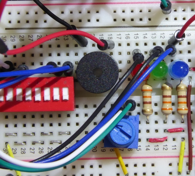
Change the Target Jump line to "circuit_4". Build the solution and program the ATmega328 flash memory. To test the program after flash programming, connect a piezoelectric buzzer between pin 11 (blue LED positive lead) of the Redboard and ground.
Note: External loads are not permitted on certain of the Redboard pins during flash programming. This includes pin 11, 12, and 13. This is why the piezoelectric buzzer cannot be connected during flash memory programming.
The configuration of the breadboard for Circuit Example 4 is pictured below.
Two things to keep in mind. The accuracy of the waveform using this method is limited by (1) the accuracy of the processor clock and (2) the value of K. We can't do much about the processor clock. We can tweak the value of K slightly up or down to compensate. K will not always calculate to a whole number. Rounding up or down will introduce a small error. Here is where choosing the largest value of N comes in handy. The larger it is, the more precise we can be making minor corrections. In a truly critical situation, we could use the 16-bit counter because our "divide by" maximum increases from 255 to 65,535 and the frequency increments decrease potentially by a factor of 65535/255 or 256! As an additional exercise, change the code to use 16-bit timer 1 and see how greater precision in frequency can be attained.
Determining the Frequency of a Waveform
Timers 0 (8-bit) and 1 (16-bit) have provision for use with an external clock. This permits them to be used as a counter. In Example 5 below, we use this feature to count external pulses for a specific time to determine the frequency of a external waveform.
Try it!
Example Circuit 5 - Measure the frequency of a waveform by using a counter/timer's external clocking input.
Assuming Example Circuit 4 is already set up to produce a known frequency (400 Hz), let's use timer 1 as a 16-bit counter to check the frequency. The basic idea will be to connect the output of timer 2 to the external clock input of timer 1, turn on the counter for one second, and read the count. The code highlighted in yellow is copied from Example Circuit 4. Added is a 10 millisecond delay to allow timer 4's output to stabilize before starting the counting.
We are ready to configure timer 1 as a simple counter. The code highlighted in green configures timer 1 in "Normal" mode and disconnects the unneeded timer 1 compare registers OC1A and OC1B from their respective pins on the Redboard. Refer to Section 20.14.1/Table 20-3 of ATmega328 Data Sheet.
Though not strictly necessary after a reset, the code highlighted in orange zeros the timer 1 count registers TCNT1H and TCNT1L. The H (high) and L (low) registers are required to accommodate the full 16 bit count. As mentioned before, we must write to them in high then low order.
The code highlighted in blue starts timer 1 with a prescale N=128, waits 1 second, then stops it. Recall that loading the TCCR I/O register with a non-zero prescaler N starts the timer/counter while a zero stops it. The remainder of code reads the timer 1 count (low and high bytes in the required order) and displays it on the ZOC terminal. Refer to Section 20.14.2/Table 20-7 of ATmega328 Data Sheet.
;
; Experiment Example Circuit 5 - Count Pulses Using 16-bit Timer/Counter
;
; Pin 11 (compare register "a" - OC2A output) connected to Pin 5 (timer 1
external input - T1)
;
circuit_5:
;
; Set Up Timer 2 to Generate 400 Hz Square Wave
;
; See Section 22 of the ATmege328 datasheet for general information
;
; See Section 22.11 specifically for register information
;
sbi
ddrb,pin11
;set port b bit 3 (pin 11) as output for OC2A
cbi ddrd,pin5
;set port d bit 5 (pin 5) as input for T1
;
; f = clk / (2 * N * K) where clk for Redboard is 16 MHz
;
ldi r16,155
;set timer 2 compare register "a" (OC2A) to K = 155 giving 400 hz frequency (See
Section 22.11.4)
;
calculated 400.64 or 0.16% error
sts ocr2a,r16
;
ldi
r16,0b01000010
;configure timer 2 for Clear Timer on Compare Match (CTC) mode and toggle OC2A
;0bxxyy00zz xx = 01 timer 2 compare register toggle OC2A output on pin 11
(See Table 22-3).
;
yy = 00 timer 2 compare register "b" not connected to pin 3 (See Table
22-6).
;
zz = 10 CTC mode See Table 22-9.
sts
TCCR2A,r16
;
; Start timer 2, the 400 Hz source
;
ldi
r16,0b00000101
;prescaler N = 128 (See Table 22-10)
sts
TCCR2B,r16
;
call
delay_10ms
;wait 10 milliseconds for a stabilized output
;
; Set Up Timer 1 To Count Pulses on T1 (pin 5)
;
; See Section 20 of the ATmege328 datasheet for general information
;
; See Section 20.14 specifically for register information
;
ldi
r16,0b00000000
;configure time 1 for normal mode as simple counter
;0bxxyy00zz xx = 00 timer 1 compare register "a" not connected to pin 9
(See Table 20-3)
; yy = 00 timer 1 compare register "b" not connected to pin 10 (See
Table 20-3)
; wzz = 000 normal mode "w" is bit 3 of tccr1b (see above)
(See Table 20-6)
sts
TCCR1A,r16
;
clr r16
;zero timer 1 count (See Section 20.14.4 and 20.14.5)
sts
TCNT1H,r16
sts
TCNT1L,r16
;
ldi
r16,0b00000110
;start timer 1 counting on external input T1 (pin 5) - clock on falling edge
(See Table 20-7)
sts
TCCR1B,r16
;
ldiw
xh,xl,1000
call delay_ms
;wait 1 second
;
lds xl,TCNT1L
;get timer 1 count
lds xh,TCNT1H
;
call crlf
;display new line
mov r16,xh
;display most significant byte (msb) of count
call decout
ldi r16,' '
;display a space
call chrout
mov r16,xl
;display least significant byte (lsb) of count
call decout
;
; Result is msb * 256 + lsb
;
circuit_5_self:
;
rjmp
circuit_5_self
;do nothing to end
Change the Target Jump line to "circuit_5". Connect pin 11 OC2A to pin 5 T1 (timer 1 external clock input). Build the solution and program the ATmega328 flash memory to test the program. Read the two values on the ZOC terminal. Multiply the first value by 256 and add the second value to get the measured frequency. We should get 001 144 or 1 * 256 + 144 = 400!
Note: Use the RESET button on the Redboard to re-run the program as needed.
The accuracy of the count is highly dependent on the one second delay, which in this case is unlikely to be very good. Using the 16-bit timer, we could count for 10 seconds to get precision to 0.1 Hz (count 4000) or even 100 seconds for two decimal places (count 40000). Of course, given the poor accuracy of the time delay, such measurement precision would be next to meaningless. Keep in mind that our object with this example was to see how to set up the ATmega328 timer to count pulses, not to build an accurate frequency counter!
Keeping Time
If we know the frequency of a waveform, we can count cycles to determine an elapsed time. We exploit this idea in Example 6 to blink an LED once per second. We also utilize the ATmega328's interrupt capability to avoid tying up the processor while waiting for the time to elapse. Below are some things to be considered when using a processor to keep time.
The AVmega328 like most modern microprocessors, provides hardware interrupt capability to handle internally or externally generated events. Here is how hardware interrupts work.
000000 940c 0035 jmp RESET ; Reset
000002 940c 0034 jmp null_int ; IRQ0
000004 940c 0034 jmp null_int ; IRQ1
000006 940c 0034 jmp null_int ; PCINT0
000008 940c 0034 jmp null_int ; PCINT1
00000a 940c 0034 jmp null_int ; PCINT2
00000c 940c 0034 jmp null_int ; Watchdog Timeout
00000e 940c 0034 jmp null_int ; Timer2 CompareA
000010 940c 0034 jmp null_int ; Timer2 CompareB
000012 940c 0034 jmp null_int ; Timer2 Overflow
000014 940c 0034 jmp null_int ; Timer1 Capture
000016 940c 00e0 jmp TIM1_COMPA ; Timer1 CompareA
000018 940c 0034 jmp null_int ; Timer1 CompareB
00001a 940c 0034 jmp null_int ; Timer1 Overflow
00001c 940c 0034 jmp null_int ; Timer0 CompareA
00001e 940c 0034 jmp null_int ; Timer0 CompareB
000020 940c 0034 jmp null_int ; Timer0 Overflow
000022 940c 0034 jmp null_int ; SPI Transfer Complete
000024 940c 0034 jmp null_int ; USART RX Complete
000026 940c 0034 jmp null_int ; USART UDR Empty
000028 940c 0034 jmp null_int ; USART TX Complete
00002a 940c 0034 jmp null_int ; ADC Conversion Complete
00002c 940c 0034 jmp null_int ; EEPROM Ready
00002e 940c 0034 jmp null_int ; Analog Comparator
000030 940c 0034 jmp null_int ; 2-wire Serial
000032 940c 0034 jmp null_int ; SPM Ready
;
null_int:
000034 9518 reti
;do nothing return (except set global interrupt flag)
Here are some considerations to keep in mind when using interrupts.
Try it!
Example Circuit 6 - Create a time base that will blink a LED once per second.
Before we use a timer interrupt, we must first set up timer 1 for CTC mode and a frequency of 1 Hz. We have two choices for N and K: N=1024 and K=7811 or N=256 and K=31,249. To gain the greatest precision for making adjustments to frequency, we choose the latter: N=256 and K=31249. See the set up code below highlighted in yellow.
Referring to section 20.14.12 of the AVmega328 Data Sheet, setting bit 1 of register TIMSK1 enables an interrupt whenever count reaches the value we loaded in compare register A. We also must set the global interrupt flag and start timer 1. See the code highlighted in blue.
The "Timer1 CompareA" JMP instruction among the interrupt vectors points to the interrupt handling routine highlighted in green. Whenever an timer event occurs (once each second), the output status of the LED is toggled. The RETI instruction returns to the main routine with the global interrupt flag set.
The main routine highlighted in orange displays on the ZOC terminal an incrementing counter in register r1 to demonstrate that the interrupts do not affect main routine processing.
;
; Experiment Example Circuit 6b - Blink Blue LED Once Per Second Using 16-bit
Timer/Counter
;
circuit_6:
;
; Set Up Timer 1
;
sbi ddrd,pin3
;set blue LED on port d bit 3 (pin 3) to output
sbi
portd,pin3
;preset blue LED on
;
; See Section 20 of the ATmege328 datasheet for general information
;
; See Section 20.14 specifically for register information
;
; f = clk / (2 * N * (1 + K)) where clk for Redboard is 16 MHz
;
ldi
r16,0b00000000 ;enable CTC for
timer 1
;0bxxyy00zz xx = 00 timer 1 compare register "a" not connected to pin 9
See Table 20-3.
; yy = 00 timer 1 compare register "b" not connected to pin 10 See
Table 20-3.
; wzz = 100 CTC mode "w" is bit 3 of tccr1b (see below) See Table 20-6.
sts
TCCR1A,r16
;
ldi
r16,high(31249) ;preset
compare register "a" to K=31,249 giving a 1 Hz interrupt
sts
ocr1ah,r16
;high byte must be written first!
ldi
r16,low(31249)
sts
ocr1al,r16
;
ldi
r16,0b00000010 ;enable timer 1
interrupt on count reaching value in compare register "a" See Section
20.14.12
;0b00000xxx xxx = 010 interrupt on count reaching value in compare register "a"
sts
TIMSK1,r16
sei
;enable global interrupt
; Main Program
;
ldi
r16,0b00001100 ;prescaler N=256;
start timer 1
sts
TCCR1B,r16
;
clr r1 ;0 ->
r1
;
circuit_6_self:
;
call
crlf
;display new line
mov
r16,r1
call
decout
;display r16 in ASCII
inc
r1
;increment r1
call
delay_1s
;delay 1 second
rjmp
circuit_6_self
;do nothing and wait for interrupts
;
; Timer 1 Interrupt Processing Routine
;
TIM1_COMPA:
;
push
r16
;save r16
in
r16, SREG
;save SREG
sbic
portd,3
;turn blue LED on if off
rjmp
TIM1_COMPA_cont0
sbi
portd,3
out
SREG, r16
;restore SREG
pop
r16
;restore r16
reti
;set global interrupt and return
;
Change the Target Jump line to "circuit_6". Connect the blue LED to pin 3 of the Redboard through a 330 ohm resister to ground. Build the solution and program the ATmega328 flash memory to test the program. Monitor the r1 counter display on the ZOC terminal to check that main processing is not affected by the timer interrupts.
Note: Using hardware interrupts leads to the most effective
use of processor resources and should be utilized whenever possible.
Producing a Pulse Width Modulated Waveform (PWM)
The ATmega328 can generate Pulse Width Modulation or PWM waveform. This is a rectangular wave of fixed frequency and controllable on-time. The percent on-time is called the duty cycle and can range from 0% to 100%. For instance, a 50% duty cycle generates a square wave. PWM waveforms are used to control servos, motors, and to do simple digital-to-analog (D/A) conversion. We demonstrate in the example below how to use PWM to control the brightness of LED's.
Try it!
Example Circuit 7 - Vary the brightness of a red, green, and blue LED in succession using PWM.
We first set up the ATmega328 for PWM. We need three timers in PSW mode, one for each LED. This requires three steps:
Step 1. Set as output pins used for PWM to output. See the code highlighted in yellow. Timers 1 and 2 have two compare registers making is possible to generate four different PWM waveforms. For this example we need only the three: two from timer 1 (compare registers A and B) and one from timer 2 (compare register A).
Step 2. Set the frequency of the rectangular wave. The Arduino uses 490 Hz, so we'll use that. We use "phase correct" mode for which the formula for frequency F is Clk/(N*510) where Clk is the Redboard's clock frequency 16 MHz and N is the prescaler value. To get approximately 490 Hz, N is 64. Refer to sections 20.14.2 and 22.11.22 of the ATmega328 Datasheet. The least three significant bits of I/O registers TCCR1B and TCCR2B control the prescaler divide by value for timers 1 and 2 respectively. According to the tables in the referenced sections, "011" and "100" select N=64 for timers 1 and 2 respectively. The remaining upper bits are zero. See the code below highlighted in green.
Note: Even though timer 1 is 16-bit, in 8-bit phase correct mode, it rolls over at 255 just like 8-bit timer 2. The frequency formula then is the same for both timers.
;
; Set Up Timer 1 for PWM Pins 9 and 10 See Section 20-14.
;
sbi
ddrb,pin9
;set port b bit 1 to output (timer 1 compare register a)
sbi
ddrb,pin10
;set port b bit 2 to output (timer 1 compare register b)
ldi
r16,0b00000011 ;prescaler clock/64 for
490 Hz
;0b00000xxx
xxx = 011 prescaler = 64 See Table 20-7.
sts
TCCR1B,r16
;
; Set Up Timer 2 for PWM for Pin 11 See Section 22-11.
;
sbi
ddrb,pin11
;set port b bit 3 to output {timer 2 compare register a)
ldi
r16,0b00000100 ;prescaler clock/64 for 490
Hz
;0b00000xxx
xxx = 100 prescaler = 64 See Table 22-10
sts
TCCR2B,r16
;
Step3. Enable PWM. I/O registers TCCR1A and TCCR2A must be configured to set up PMW. There are several possible modes, but we will use phase correct 8-bit. Refer to sections 20.14.1 (TCCR1A) and 22.11.1 (TCCR2A) of the ATmega328 Datasheet for complete details. In summary, here's how the compare registers work in phase correct mode. The compare register is loaded with the percent duty cycle desired where 0 is 0% and 255 is 100%. The timer counts up to 255 and then back down to 0 then up again. It therefore passes the compare register value twice; once counting up and again counting down. For our purposes, we have chosen to set the output to one on the down-counting match and to zero on the up counting match. The result is a 490 Hz rectangular waveform with an on-time given by the duty cycle in the compare register. See the comments in the code below for more information.
;
; Enable PWM Timer 1 See Section 20-14
;
ldi
r16,0b10100001 ;enable green and
red PWM: for timer 1, clear on compare match, and PWM phase correct
;0bxxyy00zz xx = 10 enable to clear timer 1 compare register a on
compare match when up-counting and set timer 1 compare register a on compare
match when down-counting. (pin 9) See Table 20-5.
; yy = 10 enable to clear timer 1 compare register b on
compare match when up-counting and set timer 1 compare register b on compare
match when down-counting. (pin 10) See Table 20-5.
; zz = 01 phase correct 8-bit mode
See Table 20-6
sts
TCCR1A,r16
;
; Enable PWM Timer 2
;
ldi
r16,0b10000001 ;enable blue PWM:
for timer 2, clear on compare match, and PWM phase correct
;0bxxyy00zz
xx = 10 enable to clear timer 1 compare register a on compare
match when up-counting and set timer 2 compare register a on compare match when
down-counting. (pin 11) See Table 22-5.
; yy = 00 timer 2 compare register b
disconnected See Table 22-6.
; zz = 01 phase correct 8-bit mode
See Table 22-9.
sts
TCCR2A,r16
;
This completes the PWM set up. All we need to load the compare registers at the appropriate times to send a PWM waveform voltage to the LEDs. The longer the duty cycle, the brighter the LED will appear. Below is the complete program adapted from the Redboard SIK Guide Circuit 3.
At the beginning, we turn off all the LEDs by setting their respective duty cycles to zero. The section highlighted in yellow sets up a FOR-NEXT loop with register z ranging from 0 to 768. Subroutine "showRGB" when called splits the value of z into three ranges (highlighted in green, blue, and orange) that in turn vary the duty cycle of each LED from 0 (minimum brightness) to 255 (maximum brightness). The section of code highlighted in purple loads the calculated values for each LED into the respective compare registers that sets the duty cycle and controls brightness. The 10 ms delay controls how much time each level of brightness persists.
;
; Experiment Redboard 4 - Rotate through variably bright LEDs (Analog Input)
;
circuit_7:
;
; Set Up
;
. . . See Above
;
; Main Program
;
circuit_7_again:
;
clr
r16
sts
ocr1al,r16
;preset green (pin 9) duty cycle = 0% (0 out of 255)
sts
ocr1ah,r16
sts
ocr1bl,r16
;preset red (pin 10) duty cycle = 0% (0 out of 255)
sts
ocr1bh,r16
sts
ocr2a,r16
;preset blue (pin 11) duty cycle = 0% (0 out of 255)
;
ldiw
zh,zl,0
;preset z counter to 0
;
circuit_7_loop:
;
rcall
showRGB
;showRGB(z)
call
delay_10ms
adiw
zh:zl,1
;z + 1 -> z
ldiw
xh,xl,768
;768 -> x
sub
xl,zl
;X - Z -> X
sbc
xh,zh
;
brne
circuit_7_loop
;if z <> 768, then continue looping
rjmp
circuit_7_again
;else do again from start
;
; Show RGB
;
showRGB:
push zh
;save z
push zl
;
ldiw
xh,xl,255
;255 -> x
sub
xl,zl
sbc
xh,zh
brcs
showRGB_cont0 ;if
z>255, branch to cont0
mov
r16,zl
;red = zl
clr
r17
;green = 0
clr
r18
;blue = 0
rjmp
showRGB_show ;go
show it
;
showRGB_cont0:
ldiw
xh,xl,511
;511 -> x
sub
xl,zl
sbc
xh,zh
brcs
showRGB_cont1
;if z>511, branch to cont1
clr
r16
;red = 0
ldi
r17,255
sub
r17,xl
;green=255-x
clr
r18
;blue = 0
rjmp
showRGB_show
;go show it
;
showRGB_cont1:
ldiw
xh,xl,512
sub
zl,xl
sbc
zh,xh
;zl = z - 512
clr
r16
;red = 0
clr
r17
;green = 0
mov
r18,zl
;blue = zl
;
showRGB_show:
sts
ocr1al,r16
;set red compare register
sts
ocr1bl,r17
;set green compare register
sts
ocr2a,r18
;set blue compare register
;
pop zl
;restore z
pop zh
ret
;
Change the Target Jump line to "circuit_7". Connect red, green, and blue LEDs to pins 9, 10, and 11 through 330 ohm resistors to ground. Build the solution and program the ATmega328 flash memory to test the program.
Using a BASIC Math Package
Available for the ATmega328 are math packages of various types from simple integer to extensive floating point. Included in Experiment 11 assembly code is a rudimentary 16-bit integer package. Using it is easy. Operands are always in register pairs r21 : r20 and r19 : r18 with the result returned in r21 : r20. Also included is a 16-bit version of the decimal output subroutine (dec16out) that displays r21 : r20 in decimal format. The comment code below describes the subroutines available in the package.
;
; MATH Subroutines (16 bit)
;
; Operators supported
;
; - negation: call twoComp16 with operand in r21:21;
result in r21:r20
; + addition: call add16 with operands r21:21 + r19:r19;
result in r21:r20
; - subtraction: call sub16 with operands r21:21 -
r19:r19; result in r21:r20
; * multiplication: call mul16 with operands in r21:21 *
r19:r19; result in r21:r20
; / division: call div16 with operands in r21:21 *
r19:r19; result in r21:r20
;
In Example 8 we develop a temperature display program using the TMP36 sensor included in the SparkFun Inventors Kit. The calculations needed use the subroutines in the math package.
Try it!
Example Circuit 8 - Display room temperature on the ZOC terminal.
We first connect the TMP 36. See the picture below.
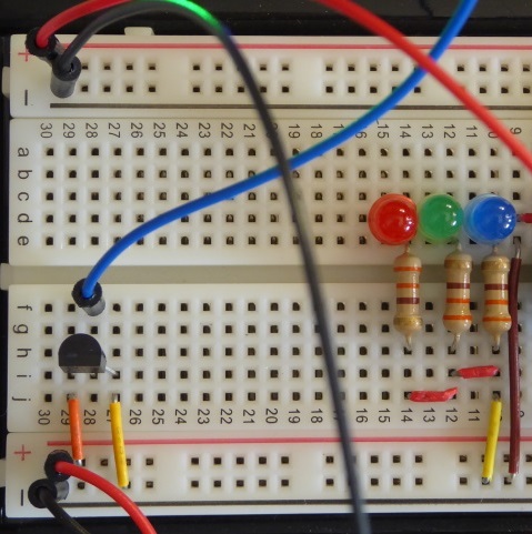
Note that the TMP 36 sensor's flat side faces the near edge of the breadboard so that the left lead connects to Vcc and the right lead connects to ground. The middle lead connects to A0 on the Redboard. Also, place a noise reducing 0.1 uF capacitor between ARef and the adjacent ground pin on the Redboard (not shown).
The first section of code is taken directly from Example 3 where we explored reading an A/D channel. After it executes, the raw A/D value of the temperature sensor is in register pair r21 : r20. The TMP 36 documentation explains that the temperature in deg C is simply the voltage output less 0.5. Our first task then is to convert the raw A/D value to voltage. Since we are working with integer arithmetic and not floating point, we subtract the 0.5 volt equivalent raw value from the sensor reading. Since 1023 represents Vcc or 5 volts, we calculate 0.5 / 5 * 1023 = 102.3 or rounded to 102 as the raw equivalent of 0.5 V. The temperature conversion then is given by T = (rawA/D - 103) * 5 / 1023.
The trick to using integer arithmetic is to determine an order of operations that keeps the result register as large as possible without exceeding its maximum value (65,535 is this case). It is also legitimate to multiply and divide by a constant and split divisors to keep the result in range. Shown below are two calculations that work in this case. The first produces the temperature to the nearest deg C as an integer. The second calculation produces a three digit result preserving the temperature to the nearest 0.1 deg C (one decimal place understood).
Temp deg C = (rawA/D - 102) * 500 / 1023 gives two digit result xx deg C. See the code below highlighted in yellow.
Temp deg C = (rawA/D - 102) * 500 / 33 * 10 / 31 gives three digit result xxx interpreted as xx.x deg C. See the code highlighted in green below.
In the latter calculation, 1023 is factored as 33 * 31 and the its division split so that the multiplication by 10 will not overflow the result. Here is the code for Example Circuit 8.
;
; Example Circuit 8 - Demonstrate Temperature Sensor
;
circuit_8:
;
; Set Up Analog-to-Digital Converter
;
ldi
r16,0b01000000
;0bxxy0zzzz xx = 01 use internal AVcc for reference (see "Table 28-3") ;
;
y = 0 right adjust result (search "Bit 5 – ADLAR")
;
zzzz = 0000 A/D channel 0 (see "Table 28-4")
sts admux,r16
;ADC Multiplexer Selection Register (search "28.9.1)
;
; Main Program
;
circuit_8_loop:
;
ldi
r16,0b11000111
;0bxy000zzz x = 1 enable A/D (search "Bit 7 – ADEN")
;
y = 1 start conversion (search "Bit 6 – ADSC")
;
zzz = 111 prescale = 128 (see "Table 28-5")
sts adcsra,r16
;ADC Control and Status Register A (search "28.9.2")
;
circuit_8_wait:
;
lds
r16,adcsra
;check if a-d conversion complete?
sbrc r16,adsc
;adsc cleared?
rjmp circuit_8_wait
;if not, wait
lds
r20,adcl
;a-d result rawA/D in r21:r20
lds
r21,adch
push r20 ;save rawA/D
push r21
ldiw
r19,r18,102
;(rawA/D - 102) * 500 / 1023 -> r21:r20 temperature to nearest deg C
call
sub16
ldiw
r19,r18,500
call
mul16
ldiw
r19,r18,1023
call
div16
set
call
dec16out ;display temperature
pop r21
;restore rawA/D
pop r20
ldiw
r19,r18,102
;(rawA/D - 102) * 500 / 33 * 10 / 31 -> r21:r20 temperature nearest 0.1 deg C
call
sub16
ldiw
r19,r18,500
call
mul16
ldiw
r19,r18,33
call
div16
ldiw
r19,r18,10
call
mul16
ldiw
r19,r18,31
call
div16
set
call dec16out
;display temperature
call crlf
;new line
ldiw xh,xl,500
;delay 500 ms
call delay_ms
rjmp circuit_8
;do again
;
Change the Target Jump line to "circuit_8". Build the solution and program the ATmega328 flash memory to test the program. Two temperature values should display on each line: the first is a two digit deg C and the second is a three digit deg C with an understood decimal point to the left of the leftmost digit.
Note: The range of temperatures obtainable depends on the calculations never over or under-flowing r21:r20. No tests were included in this example to capture such situations. The best way to handle this would be to determine the range of raw values that are permissible and test for this.
The ATmega328 has SPI (Serial Peripheral Interface) capability that can be used to communicate with a wide variety of external devices. See Section 23 of the ATmega328 Data Sheet. In summary, two SPI capable devices contain 8-bit shift registers interconnected serially. One device acts as master and clocks bytes of data from its shift register into the slave's shift register. Because the shift registers are interconnected, the slave's shift register data clocks into the master at the same time. In effect, the master's data ends up in the slave's register and the slave's data in the master's register. To read data from the slave, the master sends out a "dummy" byte (usually a zero) and reads the contents of its register after clocking is completed. The SPI slave has an instruction set that determines what is done with the master data sent. The first byte sent from master to slave after the slave is selected is read as the instruction. There may be parameter bytes that follow and even more bytes received or sent depending on the instruction. To illustrate how this works, we will interface a SPI selected EEPROM, 25LC1024. Refer to its datasheet here. (Order from Mouser #579-25LC1024-I/P) The EEPROM can store up to 131,072 (217) Bytes of 8-bit data! This EEPROM is a great storage solution for data logging.
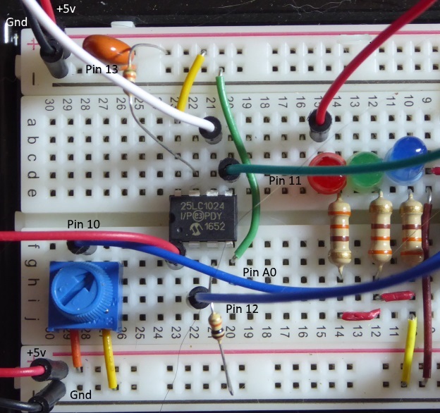
Connect the EEPROM as follows:
See the picture below. (Ignore the cat hairs on the board. These are the perils of having a long hair cat wandering over the workbench at odd hours.) Also connect the potentiometer to pin A0 (analog input channel 0) as in Example Circuit 3.
Try it!
Example Circuit 9 - Log the voltage on analog channel 0 as the potentiometer is turned. For test purposes, use 5 second logging intervals.
Note: Because this is the longest routine we have attempted so far, the code will presented and described in small sections. Refer to main.asm for a complete view of the code.
First, we create labels for the EEPROM instructions. For a detailed explanation of each, see the 25LC1024 datasheet. We will not use all of them and the ones used will be explained with the portion of code where found.
;
; 25lc1024 eeprom instruction set
;
.equ eeprom_READ = 0b00000011
.equ eeprom_WRITE = 0b00000010
.equ eeprom_WREN = 0b00000110
.equ eeprom_WRDI = 0b00000100
.equ eeprom_RDSR = 0b00000101
.equ eeprom_WRSR = 0b00000001
.equ eeprom_PE = 0b01000010
.equ eeprom_SE = 0b11011000
.equ eeprom_CE = 0b11000111
.equ eeprom_RDID = 0b10101011
.equ eeprom_DPD = 0b10111001
;
Next, we set up the SPI. The slave (EEPROM) chip select, master SPI output, and slave clock pins are set to output. See the code highlighted in yellow. The EEPROM chip select should be high, disabling the slave. See the code highlighted in orange. Lastly, the ATmega328's SPI control register SPCR must be set. See the code highlighted in green. The EEPROM specs say the maximum clock is 20 MHz. For our example, we choose a prescale divide by 16 to give a 1 MHz clock. Other faster clock settings are available. See Table 23-5.
;
; Set Up SPI
;
ldi r16,0b00101100
;port b bits 2 (CS), 3 (MOSI), and 5 (SCK) as output ;
out
ddrb,r16
;update data direction register B
sbi
portb,2
;deselect eeprom
ldi
r16,0b01010001
;0btuvwxyzz t = 0 disable SPI interrupt (See section 23.5.1)
; u = 1 enable SPI
; v = 0 least significant bit (LSB) first
; w = 1 select ATmega328 as master
; xx = 00 SPI mode 0
; zz = 01 clock prescale = 16 for SPI clock = 1 Mhz (see "Table 23-5")
out
spcr,r16
;configure SPI control register
;
The analog channel is set up exactly as in Example Circuit 3.
;
; Set Up Analog-to-Digital Converter
;
ldi
r16,0b01000000
;0bxxy0zzzz xx = 01 use internal AVcc for reference (search "Table 28-3")
; y = 0 right adjust result (search "Bit 5 – ADLAR")
; zzzz = 0000 A/D channel 0 (see "Table 28-4")
sts admux,r16
;
The most basic task is to write and read a single byte over the SPI channel. The subroutine for writing is "spi_write". See below. Provided the Atmega328's SPI in enabled, simply writing to I/O register SPDR sends the byte in the designated register (R16) over the serial link (MOSI). See the code highlighted in yellow. The code enters a wait until the SPIF bit (bit 7) of I/O register SPSR is set indicating that the write cycle is completed. See the code highlighted in orange. After which, the subroutine returns to the calling program.
To read a slave byte, we have to send a "dummy" byte to the slave. We do this at the beginning of "spi_read" below with the "dummy" byte a zero. See the code highlighted in green. As before, we wait for the write cycle to finish, but this time, we read the SPDR I/O register into R16 before return. See the code highlighted in blue. Recall that while clocking out the "dummy" byte, the contents of the slave's shift register was clocking the other direction into the ATmega328's shift register.
Note: Neither subroutine selects the slave. We will do this subroutines that issue instructions to the slave.
;
; SPI Write r16
;
spi_write:
;
out
spdr,r16
;send byte to SPI
;
spi_write_wait:
;
in
r16,spsr
;write completed?
sbrs
r16,spif
;if not, wait
rjmp
spi_write_wait
ret
;
; SPI Read into r16
;
spi_read:
;
ldi
r16,0
;send dummy byte to spi
out
spdr,r16
;
spi_read_wait:
;
in
r16,spsr
;write completed?
sbrs
r16,spif
;if not, wait
rjmp
spi_read_wait
in
r16,spdr
;get return byte
ret
A good example of a simple read is getting the electronic signature (ID) from the EEPROM. The datasheet for the 25LC1024 indicates is "41". Here are the steps to read it.
Select the slave by clearing pin 10 (port b bit 2). See the code highlighted in yellow.
Write the RDID (Read ID) instruction to the EEPROM. See the code highlighted in orange.
Write a dummy 24-bit address as three zero bytes. See the code highlighted in green.
Read the electronic signature, deselect the EEPROM, and return with it in R16. See the code highlighted in blue.
Reading and checking the electronic signature is a good way to be sure the SPI device is connected and working
;
; SPI Read Electronic Signature
;
circuit_9_esig:
;
cbi
portb,2
;select eeprom
ldi
r16,eeprom_RDID
;send esig request
rcall
spi_write
;
ldi
r17,3
;send 3 dummy 24-byte address
;
circuit_9_esig_loop:
;
ldi
r16,0
rcall
spi_write
dec
r17
;done?
brne
circuit_9_esig_loop
;if not, loop
;
rcall
spi_read
;read esig
sbi
portb,2
;deselect eeprom
ret
We also need to read the EEPROM status register SDSR after writing data bytes. We can write as many as 256 bytes at a time, but we must wait for the actual write cycle to complete before reading back what is written. After reading the status register, we check to see that bit 0 (WIP Write In Progress) has cleared indicating that the write cycle is completed. In the code below, we select the EEPROM (yellow), write the read status instruction RSDR (orange), read the status byte into R16 (green), deselect the EEPROM, and return (blue).
;
; SPI Read Status Register into r16
;
spi_read_SDSR:
;
cbi
portb,2
;select eeprom
ldi
r16,eeprom_RDSR
;send status register read request
rcall
spi_write
rcall
spi_read
;read status register
sbi
portb,2
;deselect eeprom and start write cycle
ret
The analog data we plan to store in the EEPROM requires two bytes, the write and read EEPROM subroutines handle a word (double byte).
Specifying the address in the EEPROM requires some explanation. The address space of the 25LC1024 is 0x00000 to 0x01FFFF or 512 pages of 256 bytes per page. The maximum number of bytes that can be written in any one write cycle is 256. Writing across a page boundary is prohibited. A good strategy for addressing then is to store data by page beginning at page 0 (0x000) and ending at page 511 (0x1FF), never writing more than 256 bytes per page. In the SPI Write Word subroutine below, registers R26 and R25 contain the startingpage and R24, the starting location.
The "SPI Write Word" code below is self-explanatory for the most part. Registers R26:R25:R24 contains the starting address. Registers R21:R20 contain the word (double byte) to be stored in the EEPROM. One point, a write enable instruction must be sent prior to a write cycle. See the code highlighted in yellow. Also, the 24-bit address is sent most significant byte first (immediately after the write instruction). See the code highlighted in orange. And lastly, after writing the last byte and deselecting the EEPROM, the status register is checked for the Write-In-Progress bit to have cleared indicating the bytes have been written and verified.
;
; SPI Write Word (Double Byte)
;
; r21:r20 contains the word to written
; r26:r25:R24 contain the 24-bit address
;
circuit_9_write_word:
;
cbi
portb,2
;select eeprom
ldi
r16,eeprom_WREN
;send write enable request
rcall
spi_write
sbi
portb,2
;deselect eeprom
cbi
portb,2
;select eeprom
ldi
r16,eeprom_WRITE
;send write request
rcall
spi_write
mov r16,r26
;send 24-bit address
rcall
spi_write
mov r16,r25
rcall
spi_write
mov r16,r24
rcall
spi_write
mov r16,r21
;send most significant byte to be written
rcall
spi_write
mov r16,r20
;send least significant byte to be written
rcall
spi_write
sbi
portb,2
;deselect eeprom and start write cycle
;
circuit_write_word_wait:
;
rcall
spi_read_SDSR
;read status register
sbrc r16,0
;wait while WIP bit 0 set (write in progress)
rjmp
circuit_write_word_wait
ret
;
The "SPI Read Word" subroutine below is equally straightforward. After writing the READ instruction to the EEPROM, the 24-bit address is sent. Each subsequent "spi_read" call brings a stored byte in sequence. Registers R21:R20 return with word (double byte) stored in the EEPROM.
;
; SPI Read Word (Double Byte)
;
; r21:r20 contains the byte read
; r26:r25:R24 contain the 24-bit address
;
circuit_9_read_word:
;
cbi
portb,2
;select eeprom
ldi
r16,eeprom_READ
;send read request
rcall
spi_write
mov r16,r26
;send 24-bit address
rcall
spi_write
mov r16,r25
rcall
spi_write
mov r16,r24
rcall
spi_write
rcall
spi_read
;read most significant byte
mov r21,r16
rcall
spi_read
;read least significant byte
mov r20,r16
sbi
portb,2
;deselect eeprom
ret
;
Putting it altogether, the main program is shown below. The principle sections are highlighted in color below.
Get, check, and display the electronic signature of the 25LC1024. See the code highlighted in yellow.
Set up for ten iterations and establish starting address for EEPROM storage for writing raw A/D values to EEPROM. See the code highlighted in orange.
Read and store the A/D value (setting of potentiometer) then continue to next iteration. See the code highlighted in green.
Set up for ten iterations and establish starting address for EEPROM storage for reading stored raw A/D values from EEPROM. See the code highlighted in blue.
Read and display for verification the raw A/D values previously stored in the EEPROM. See the code highlighted in purple.
;
; Example Circuit 9 - Demonstrate SPI Communication
;
. . .
;
circuit_9:
;
. . .
;
; Main
;
rcall crlf
;display new line
rcall
circuit_9_esig
;get esig
cpi
r16, 41
; 41?
breq
circuit_9_cont0
;if so, continue
ldiw zh,zl,(spi_error_esig<<1)
;point z register to start of error message
rcall msgout
;display error message
call
crlf
rjmp circuit_9_self
;
circuit_9_cont0:
;
push r16
;save r16
ldiw
zh,zl,(spi_msg_0<<1)
;point z register to start of message 0
rcall
msgout
;display esig message
pop r16
;restore r16
set
rcall decout
;display electronic signature
rcall crlf
;display new line
;
; Write Raw A/D Data to EEPROM
;
ldiw zh,zl,(spi_msg_1<<1)
;point z register to start of message 0
rcall msgout
;display Raw A/D write message
rcall crlf
;display new line
ldi
r16,10
;set max iterations to 10
mov r3,r16
clr
r4
;set count to 0
;
ldiw
r26,r25,0
;set page of 24-bit starting address
ldi
r24,0
;set location of 24-bit starting address
;
circuit_9_loop0:
;
ldi
r16,0b11000111
;0bxy000zzz x = 1 enable A/D (search "Bit 7 – ADEN")
; y = 1 start conversion (search "Bit 6 – ADSC")
; zzz = 111 prescale = 128 (seeearch "Table 28-5")
sts
adcsra,r16
;ADC Control and Status Register A (search "28.9.2")
;
circuit_9_wait:
;
lds
r16,adcsra
;check if a-d conversion complete?
sbrc r16,adsc
;adsc cleared?
rjmp
circuit_9_wait
;if not, wait
lds
r20,adcl
;a-d result rawA/D in r21:r20
lds
r21,adch
rcall
circuit_9_write_word
;write raw A/D to eeprom
mov r16,r4
;display count
clt
rcall decout
inc
r4
;increment count
set
call
dec16out
;display raw A/D
call
crlf
;display new line
rcall delay_5s
;5 second delay
addi r24,2
;bump to next address in eeprom
dec r3
;done?
brne circuit_9_loop0
;if not, loop
;
rcall crlf ;display
new line
;
; Read Data Back from EEPROM
;
ldiw zh,zl,(spi_msg_2<<1)
;point z register to start of message 0
rcall msgout
;display Raw A/D read message
rcall crlf
;display new line
ldi
r16,10
;set max iterations to 10
mov r3,r16
clr
r4
;set count to 0
ldiw
r26,r25,0
;set page of 24-bit starting address
ldi
r24,0
;set location of 24-bit starting address
;
circuit_9_loop1:
;
mov r16,r4
;display count
clt
call
decout
inc
r4
;increment count
rcall
circuit_9_read_word
;read raw A/D from eeprom
set
;display it
rcall
dec16out
rcall crlf
;display new line
addi r24,2
;bump to next address in eeprom
dec r3
;done:
brne
circuit_9_loop1
;if not, loop
;
circuit_9_self:
;
jmp
circuit_9_self
;
. . .
;
spi_msg_0: .db "25LC1024 EEPROM Electronic Signature: ", 0, 0
spi_msg_1: .db "Raw A/D Data Written to EEPROM: ", 0, 0
spi_msg_2: .db "Data Read Back from EEPROM: ", 0, 0
spi_error_esig: .db "SPI Error: Wrong electronic signature",0
spi_error_wel: .db "SPI Error: Write enable latch not set",0
;
Change the Target Jump line to "circuit_9".
Build
the solution and program the ATmega328 flash memory to test the program. Watch
the values written to and read back from the EEPROM on the ZOC terminal.
Change the page of the EEPROM address and rerun the program.
This completes exploration of ATmega328 peripherals.