Experiment 9 - ATmega328 Selection and Branching
In this experiment, we continue to explore the ATmega328 using the basic knowledge we acquired working with the Intel 8080. Follow the procedure in Experiment 8 (see here) for setting up an ATMEL Studio project called "Experiment_9". Use the "main.asm file here.
Experiment 9-0 - Input/Output Capability with the ATmega328
The Intel 8080 has no internal digital I/O ports; all are external, usually on separate "parallel I/O" boards that communicate with the processor board via a buss like the S-100. The ATmega328, on the other hand, has three internal digital I/O ports designated "PORTB", "PORTC", and "PORTD". PORTB and PORTD are 8-bit; PORTC is 7-bit. Individual bits of these ports can function as simple digital I/O or, with appropriate configuration, perform functions associated with ATmega328's internal peripherals (counter/timers, serial I/O, analog to digital converters, etc.).
Intel 8080 S-100 peripheral boards are generally hardware configured using wire jumpers. The ATmega328's I/O peripherals are software configured using I/O registers. For instance, to use ATmega328 ports for digital I/O, we output configuration data to DDRn, the data direction I/O register where n is A, B, or C. Recall there are 64 I/O registers numbered 0 to 63. DDRB is I/O register 4, DDRC is I/O register 7, and DDRD is I/O register 10. For convenience, the ATmega328 assembler keeps track of I/O register numbers so we can reference them with mnemonics like "DDRB".
One nice feature of the ATmega328 when using it for Digital I/O is that any bit on any port can be configured as input or output. Setting a bit in a DDRn register makes it an output; clearing it makes it an input. For our code testing, we make all bits of ports B and C input by clearing all bits of the DDRB and DDRC I/O registers. See the lines highlighted in yellow in the I/O configuration code below. The ATmega328 has configurable pull-up resistors that can be activated by setting bits on PORTB and PORTC I/O registers. See the lines highlighted in blue below. Lastly, to use PORTD to drive the Data LEDs, we set all bits of DDRD. See the lines highlighted in green below.
;
; I/O Configuration Code
;
ldi
r16,0b00000000 ;set all bits of port b
to input
out ddrb,r16
ldi
r16,0b11111111 ;turn on pull-up
resistors on all bits of PORTB
out
PORTB,r16
ldi r16,0b00000000
;set all bits of port c to input
out ddrc,r16
ldi r16,0b11111111
;turn on pull-up resistors on all bits of port c
out
PORTC,r16
ldi r16,0b11111111
;set all bits of port d to output
out ddrd,r16
Once configured, we use the IN and OUT instructions to perform input and output on the ATmega328's external pins. While the ATmega328's IN and OUT instructions are similar to the Intel 8080, there are a couple of differences: (1) The Intel 8080 transfers data to and from the A register only while the ATmega328 can utilize any register R0 to R31 and (2) The Intel 8080 can address up to 256 ports (0 to 255) while the ATmega328 IN and OUT instructions up to 64 ( 0 to 63). Here are the specifics:
| Basic Operation Example | Intel 8080 | ATmega328 |
| Input from input port to a register | IN p where p = 0 to 225 Data value on port "p" transferred to register A |
IN Rn,
PINx where n = 0 to 31 & x = a, b, or c Data value on port "x" transferred to register "n" |
| Output from a register to output port | OUT p where p = 0 to 225 Data value in register A transferred to port "p" |
OUT PORTx, Rn where n = 0 to 31 &
x = a, b, or c Data value in register "n" transferred to port "x" |
Try it!
Experiment 9-4 Example 1. Code a basic I/O routine that inputs from the Sense Switches and outputs to the Data LEDs.
The ATmega328 code in this example is essentially the same as the Intel 8080 except that we must specify a destination register, in this case r16. Also note that the Redboard sense switches connect to PORT B bits 0 to 5, so this direct I/O test only affects these bits. See the code comments for more specifics.
;
; Experiment 4 Example 1 - Basic I/O
;
; Using IN and OUT instructions
;
; Set Sense Switches to 0b00xxxxxx (any one or more x's set and all others
closed)
;
; Data LEDs display complement pattern
;
; Note: (1) Bits 0 to 5 of PORT B connect directly to senses switches 1 to 6. Sense
switches 7 and 8 are connected
; to bits 1 and 2 of PORTC. (2) When inputting sense switch PORTB directly, "up"
produces cleared (0) bit while "down" a
; set (1) bit. (3) While programming flash memory, all sense switches must be
"down"; i.e., open.
;
exmp4_1:
in
r16,pinb
;get lower six bits of Sense Switches on port b
out
portd,r16
;update LEDs on port d
rjmp
exmp4_1
;repeat
;
Change the Target Jump line to "exmp4_1". Build the solution and program the ATmega328 flash memory to test the program.
Note: As mentioned previously, the sense switches are not the same as on the Altair simulation: up is closed and produces a zero, not a one. The decision to arrange the DIP switch this way was made to avoid a flash programming issues when the DIP switches were in their "normal" down position.
Change the "in" statement to reference "pinc". Redo the example and see that sense switches 7 and 8 affect the lsft most LEDs as they are connected to bits 0 and 1 of PORTC. Examine the "ssinp" subroutine and see that these two bits are rotated into bits 6 and 7 then ORed with the lower six bits from PORTB to form the final sense switch value in register r16.
It should be clear now why we had to use a subroutines to make our the Redboard sense switches function like the Altair.
Experiment 9-4 Selection and Branching
For the Intel 8080, a program can "jump" conditionally or unconditionally to any address in the Intel 8080's 64K address space. Intel 8080 "jump" instructions require three bytes of 8-bit program memory: one for the instruction and two for the 16 bit address.
Likewise, the ATmega328 has an unconditional jump instruction "JMP" that can reach anywhere in its 32K program address space. "JMP" requires two 16-bit words of program memory: one for the instruction and one for the 16 bit address. The designers of the ATmega328 recognized that conditional jumps were frequently to "near by" addresses, not requiring a full 16-bit address. With this in mind, they developed a collection of "branch" instructions that perform a relative jump to the address PC + 1 + k where -64 < k < 63. Using the assembler, we simply designate the label and the assembler calculates k. If we try to branch beyond the limits of k, an assembly error is generated.
The first two tables below compare the Intel 8080 and ATmega328 jump instructions instructions. The remaining tables describe additional branching instructions available only with the ATmega328.
| Unconditional Branching | |||
| 8080 JUMP Instruction |
ATmega328 Instruction |
ATmega328 Status Bit |
Comment |
| JMP | JMP K | Unconditional Jump to address K where 0 ≤ K< 4M* -> PC (Requires 2 16-bit words) | |
| N.A. | RJMP k | Unconditional Relative jump to an address within PC - 2K +1 and PC + 2K (Requires 1 16-bit word) | |
| PCHL | IJMP | Indirect Unconditional Jump to address in 16-bit Z register (R31:R30) -> PC ** (Requires 1 16-bit word) | |
| Conditional Branching - Unsigned Numbers | |||
| 8080 JUMP Instruction |
ATmega328 Instruction |
ATmega328 Status Bit |
Comment |
| JNZ | BRNE k | Z = 0 | Branch if not equal (signed or unsigned) If the instruction is executed immediately after any of the instructions CP, CPI, SUB, or SUBI, the branch will occur if and only if, the unsigned or signed binary number represented in Rd was not equal to the unsigned or signed binary number represented in Rr. |
| JZ | BREQ k | Z = 1 | Branch if equal (signed or unsigned) If the instruction is executed immediately after any of the instructions CP, CPI, SUB, or SUBI, the branch will occur if and only if the unsigned or signed binary number represented in Rd was equal to the unsigned or signed binary number represented in Rr. |
| JNC | BRSH k | C = 0 | Branch if same or higher (unsigned) If the instruction is executed immediately after execution of any of the instructions CP, CPI, SUB, or SUBI, the branch will occur if and only if, the unsigned binary number represented in Rd was greater than or equal to the unsigned binary number represented in Rr. |
| JC | BRLO k | C = 1 | Branch if lower (unsigned) If the instruction is executed immediately after any of the instructions CP, CPI, SUB, or SUBI, the branch will occur if and only if, the unsigned binary number represented in Rd was smaller than the unsigned binary number represented in Rr |
| JPO | N.A. | ||
| JPE | N.A. | ||
| JP | BRPL k | N = 0 | Branch on plus |
| JM | BRMI k | N = 1 | Branch on minus |
* For the ATmega328, K is limited to the flash memory
space 32,767.
** For the ATmega328, Z is limited to the flash memory space 32,767.
| Additional ATmega328 Conditional Branching - Signed Numbers | ||
| ATmega328 Instruction |
ATmega328 Status Bit |
Comment |
| BRGE k | N eor V = 0 | Branch if greater or equal (signed) If the instruction is executed immediately after any of the instructions CP, CPI, SUB, or SUBI, the branch will occur if and only if the signed binary number represented in Rd was greater than or equal to the signed binary number represented in Rr. ("eor" = Exclusive OR) |
| BRLT k | N eor V = 1) | Branch if less than (signed) If the instruction is executed immediately after any of the instructions CP, CPI, SUB, or SUBI, the branch will occur if and only if, the signed binary number represented in Rd was less than the signed binary number represented in Rr. ("eor" = Exclusive OR) |
Note: BRSH and BRLO above work with
unsigned binary numbers. BRGE and BRLT
work with signed binary numbers.
| Additional ATmega328 Conditional Branching - Based on Status Register Values | ||
| ATmega328 Instruction |
ATmega328 Status Bit |
Comment |
| BRBC b,k | Branch if bit b in status register is cleared b = 0 C, 1 Z, 2 N, 3 V, 4 S, 5 H, 6 T, 7 I | |
| BRBS b,k | Branch if bit b in status register is set b = 0 C, 1 Z, 2 N, 3 V, 4 S, 5 H, 6 T, 7 I | |
| BRCC k | C = 0 | Branch on carry cleared |
| BRCS k | C = 1 | Branch on carry set |
| BRHC k | H = 0 | Branch on half-carry cleared |
| BRHS k | H = 1 | Branch on half-carry set |
| BRID k | I = 0 | Branch on global interrupt disabled |
| BRIE k | I = 1 | Branch on global interrupt enabled |
| BRTC k | T = 0 | Branch on T cleared |
| BRTS k | T = 1 | Branch on T set |
| BRVC k | V = 0 | Branch on V cleared |
| BRVS k | V = 1 | Branch on V set |
Finally, the ATmega328 has four test instructions that skip the next instruction if a certain condition is met.
| ATmega328 Conditional Branching - Skip Next Instruction | |
| ATmega328 Instruction |
Comment |
| SBIC A,b | Skip next instruction if bit b in I/O register A is cleared |
| SBIS A,b | Skip next instruction if bit b in I/O register A is set |
| SBRC Rr,b | Skip next instruction if bit b in working register Rr is cleared |
| SBRS Rr,b | Skip next instruction if bit b in working register Rr is set |
| CPSE Rd,Rr | Skip the next instruction if registers Rd and Rr are equal |
Note: When using "Skip Next Instructions" in loops, create the loop with the "next instruction" so that the skip only occurs when the condition is met. This provides the fastest execution.
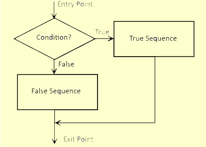
Two Way and One Way Selection
Recall the basic flow diagrams for selection.
| TWO-WAY SELECTION |
|
|
| ONE-WAY SELECTION |
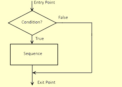 |
The ATmega328 selection scheme is basically the same as the Intel 8080 with the former's conditional branching instructions replacing the latter's conditional jump instructions.
Try it!
Experiment 9-4 Example 2. Display a one in the Data LEDs if bit 7 in the sense switches is set or a zero if it is cleared.
The code as implemented below explores two way selection using a logical operation (AND). As required, the branch and relative jump instructions are "nearby" and within the specified ranges of k.
;
; Experiment 4 Example 2 - Two Way Selection (mask condition)
;
; Setting sense switch bit 7 = 1 displays a one (true) in Data LEDs.
Otherwise, zero (false) is displayed.
;
exmp4_2:
call
ssinp
;get Sense Switches into R16
andi
r16,0b10000000 ;mask r16 to test bit 7
brne exmp4_2_true
;if r16 bit 7 = 1, branch to true sequence
;
; False sequence
;
ldi
r16,0
;load zero (false) in r16
rjmp exmp4_2_exit ;branch to exit
;
; True sequence
;
exmp4_2_true:
ldi
r16,1
;load one (true) in r16
;
; Exit
;
exmp4_2_exit:
call LEDout
;display r16 in Data LEDs
rjmp exmp4_2 ;repeat
Change the Target Jump line to "exmp4_2". Build the solution and program the ATmega328 flash memory to test the program.
Experiment 9-4 Example 3. Like Example 2 above, the code below tests bit 7 of the sense switch only it uses a one way selection approach. The first code sequence (3a) duplicates the Intel 8080 code closely. The second (3b) simplifies the code by using the skip instruction (SBIS) that looks directly at the I/O bit (PORTC pin 1) and, if set, skips the next instruction.
;
; Experiment 4 Example 3a - One Way Selection (mask condition)
;
; Sense switch bit 7 = 1 will produce a one (true) in Data LEDs
;
exmp4_3a:
call
ssinp
;get Sense Switches into R16
andi
r16,0b10000000 ;mask r16 to test
bit 7
ldi
r16,0
;preload r16 with zero (false)
breq
exmp4_3a_exit
;if r16 bit 7 = 0, branch to exit
;
; True sequence
;
ldi
r16,1
;load one (true) in r16
;
; Exit
;
exmp4_3a_exit:
call LEDout ;display r16 in Data LEDs
rjmp exmp4_3a
;repeat
;
; Experiment 4 Example 3b - One Way Selection (mask condition using skip
instruction)
;
; Sense switch bit 7 = 1 will produce a one (true) in Data LEDs
;
; Reads I/O port c pin (bit) 1 directly. Recall that Sense Switch 7 up produces
a zero on PORTC bit 1
;.
exmp4_3b:
ldi
r16,0 ;preload
r16 with zero (false)
sbis pinc,1
;if PORTC pin (bit) 1 = 1 (sense switch down), skip next instruction and go to exit
;
; True sequence
;
ldi
r16,1
;load one (true) in r16
;
; Exit
;
exmp4_3b_exit:
call
LEDout ;display r16 in Data LEDs
rjmp
exmp4_3b ;repeat
Change the Target Jump line to "exmp4_3a". Build the solution and program the ATmega328 flash memory to test the program. Repeat for "exmp4_3b".
Arithmetic Branching with the ATmega328
The ATmega328 provides for both unsigned and signed arithmetic selection; the Intel 8080 has only unsigned arithmetic selection. This is a welcomed addition and provides more convenient handling of arithmetic conditioning with signed numbers.
Try it!
Experiment 4 Example 4. With the code below, we explore unsigned and signed arithmetic comparison. In example 4a, input from the Sense Switches is compared to the number 80 using the unsigned branch instruction BRSH (branch on Same or Higher). We display in the Data LEDs either a one for True or zero for False. Example 4b, demonstrates that signed branching with BRGE (branch on Greater of Equal) works equally well with signed numbers like -80. Finally, in Example 4c, we achieve modest simplification by using a one-way selection.
;
; Experiment 4 Example 4a - Two Way Selection (unsigned comparison)
;
; Any sense switch input equal or greater than 120Q will produce a one (true)
;
exmp4_4a:
call
ssinp
;get Sense Switches into R16
cpi
r16,80
;compare r16 to 80 (r16 - 80)
brsh
exmp4_4a_true ;if r16 >= 80 branch to true sequence
;
; False sequence
;
ldi
r16,0
;zero (false) -> r16
rjmp exmp4_4a_exit
;branch to exit
;
; True sequence
;
exmp4_4a_true:
ldi
r16,1
;one (true) -> r16
;
; Exit
;
exmp4_4a_exit:
call LEDout
;display r16 in Data LEDs
rjmp exmp4_4a
;repeat
;
; Experiment 4 Example 4b - Two Way Selection (signed comparison)
;
; Try these sense switch settings: (1) 000Q = 0 >= -80 LEDs = 1 (True)
; (2) 261Q = -79 >= -80 LEDs = 1 (True)
; (3) 260Q = -80 >= -80 LEDs = 1 (True)
; (4) 257Q = -81 < -80 LEDs = 0 (False)
;
exmp4_4b:
call
ssinp
;get Sense Switches into R16
cpi
r16,-80
;compare r16 to -80 (r16 - (-80))
brge
exmp4_4b_true ;if r16 >= -80 branch to true sequence
;
; False sequence
;
ldi
r16,0
;zero (false) -> r16
rjmp
exmp4_4b_exit ;branch to exit
;
; True sequence
;
exmp4_4b_true:
ldi
r16,1
;one (true) -> r16
;
; Exit
;
exmp4_4b_exit:
call
LEDout
;display r16 in Data LEDs
rjmp exmp4_4b
;repeat
;
; Experiment 4 Example 4c - One Way Selection (unsigned comparison)
;
; Any sense switch input less than 80 will produce a zero (false)
;
exmp4_4c:
call
ssinp
;get Sense Switches into r16
cpi
r16,80
;compare r16 to 80 (r16 - 80)
ldi
r16,0
; (preload) zero (false) -> r16
brlo
exmp4_4c_exit ;if r16 < 80 branch to exit
;
; True sequence
;
ldi
r16,1
;one (true) -> r16
;
; Exit
;
exmp4_4c_exit:
call LEDout
;display r16 in Data LEDs
rjmp exmp4_4c
;repeat
;
Change the Target Jump line to "exmp4_4a". Build the solution and program the ATmega328 flash memory to test the program. Repeat for "exmp4_4b" and "exmp4_4c".
Experiment 9-4 Example 5. In Example 5 we use arithmetic comparison in a one-way selection to switch values in two registers and display the larger of two. One value is entered in the Sense Switches (via r16) and the other a constant value 120 (via r17). Rather than compare immediate, we use the register compare instruction CP. Register r1 is used as a temporary register for switching r16 and r17.
;
; Experiment 4 Example 5 - One Way Selection (arithmetic comparison - unsigned)
;
; Display the larger of 120 (170Q) and the value in the Sense Switches
;
exmp4_5:
ldi
r17,120
;load r17 with 120
call
ssinp
;load r16 with sense switch value
cp
r17,r16
;compare r17 to r16 (120 - r16)
brlo
exmp4_5_exit ;if r16 < 80 branch to exit
;
; True sequence - Switch registers
;
mov
r1,r16
;r16 -> r1 (temporary register)
mov
r16,r17 ;r17
-> r16
mov
r17,r1
;r1 -> r17
;
; Exit
;
exmp4_5_exit:
call
LEDout
;display r16 in Data LEDs
rjmp exmp4_5
;repeat
Change the Target Jump line to "exmp4_5". Build the solution and program the ATmega328 flash memory to test the program.
Experiment 9-4 Example 6. In Example 6 we convert the lower hex nibble in the Sense Switches to ASCII and display the latter in the Data LEDs.
;
; Experiment 4 Example 6 - One Way Selection
;
; Convert the low nibble of the Sense Switches from hex to ASCII
;
exmp4_6:
call
ssinp
;load r16 with sense switch value
andi r16,
0x0f
;mask off upper nibble
addi r16,48
;assume value 0 to 9 and add 48 ASCII bias
cpi
r16,57
;if r16 < 57, branch to exit
brlo
exmp4_6_exit
;
; True sequence
;
addi r16,7
;add 7 more ASCII bias for values 10 to 15
;
; Exit
;
exmp4_6_exit:
call LEDout
;display r16 in Data LEDs
;0000 - ASCII 0 or 060Q to 1001 - ASCII 9 or 101Q
;1010 - ASCII A or 101Q to 1111 - ASCII F or 106Q
rjmp exmp4_6
;repeat
Change the Target Jump line to "exmp4_6". Build the solution and program the ATmega328 flash memory to test the program.
Continue to next Experiment - Click Here