
Experiment 10 - ATmega328 Iteration
In this experiment, we continue to explore the ATmega328 using serial I/O and a terminal rather than Sense Switches and LEDs. Follow the procedure in Experiment 8 (see here) for setting up an ATMEL Studio project called "Experiment_10". Use the "main.asm file here.
Experiment 10-0 Serial Input/Output Capability with the ATmega328
Included in the internal peripherals of the ATmega328 is a universal serial transmitter/receiver or USART. We will use the USART to communicate with a PC terminal emulator giving us keyboard and screen display capability.
The USART is assigned specific I/O registers. These are describe in detail in Section 24.12 of the Atmega328 Datasheet. The chart below provides a brief explanation of each of the I/O registers.
| I/O Register | Address | Purpose | Instruction* |
| UDR0 | 0xC6 = 198 | Transmit and receive data buffer. Data to be transmitted or data received written to or read from this register. See Section 24.12.1 | STS or LDS |
| UCSR0A | 0xC0 = 192 | Control and status register A. Determine when receive and transmits are complete plus others. See Section 24.12.2 | STS or LDS |
| UCSR0B | 0xC1 = 193 | Control and status register B. Enable USART transmit and receive plus others. See Section 24.12.3 | STS or LDS |
| UCSR0C | 0xC2 = 194 | Control and status register C. Set mode, parity, number of stop and data bits, etc. See Section 24.12.4 | STS or LDS |
| UBRR0L UBRR0H |
0xC4 = 196 0xC5 = 197 |
Baud rate registers (low and high bytes). For 16 MHx clock see Table 24-7 | STS or LDS |
* Note: For I/O registers in the range of 0x00 to 0x3F (0 to 63) use the IN and OUT instruction. Beyond this range use the LDS and STS instructions. The assembler assumes that if we access I/O registers 0 to 63, we will use IN and OUT. If we use LDS and STS with the 0 to 63 we have to include the offset 0x20 or we get the wrong I/O register. By following the preceding rule, we don't have to worry about this.
In Experiment 9 we configured 8-bit PORTS B, C, and D for digital I/O. For serial I/O, PORTD bit 1 as output for serial transmit (TXD) and PORTD bit 0 as input for serial receive (RXD). Enabling Rx and Tx overrides the data direction of pins 0 and 1 on the Redboard, so configuring the data direction register is unnecessary. Three programming steps are required to configure the USART for basic serial I/O: (1) Enable the USART transmitter and receiver (highlighted in blue), (2) Set the baud rate (highlighted in yellow), and (3) Set the frame format (highlighted in green). For the latter two, we use 9600 baud with 8 data bit and 2 stop bits. The values for configuration constants in the code below can be gleaned from reviewing section 24 of the ATmega328 Datasheet.
; Baud Rate
;
.equ ubrrval = 103
;See Table 24-7 fosc = 16 Mhz U2Xn = 0 column
;
start:
;
; Enable Transmit and receive See Section 24.12.3
;
ldi r16,
0b00011000
;0buuuvwxyz uuu = 000 disable all USART interrupts (Search "Bit 7 –
RXCIE0")
;
v =
1 enable Rx (receive) (Search "Bit 4 – RXEN0")
;
w =
1 enable Tx (transmit) Search "Bit 3 - TXEN0")
; x = 0
selects number of character bits less than nine. Associated with UCSZ00 and
UCSZ01 in I/O register UCSR0C (Search "Bit 2 - UCSZ02")
;
y = 0 ninth received bit if x = 1. (Search "Bit 1 - RXB80")
;
z = 0 ninth transmit bit if x = 1 (Search "Bit 1 - TXB80")
sts ucsr0b,r16
;
; Baud Rate 9600
;
ldi r17, HIGH(ubrrval)
;UBRR High
ldi r16, LOW(ubrrval)
;UBBR Low
sts ubrr0h,r17
sts ubrr0l,r16
;
; Frame Format: 8 data, 2 stop, no parity
;
ldi
r16, 0b000001110
;0buuvvwxxy uu = 00 select asynchronous USART mode (Ses Table 24-8)
;
vv = 00 disable parity (See Table 24-9)
;
w = 1 select 2 stop bits (Search "Bit 3 - USBS0")
;
xx = 11 selects 8 data bit. Associated with UCSZ02 in I/O register UCSR0B
(Search "Bit 2 - UCSZ01")
;
y = 0 for asynchronous mode. (Search "Bit 0 - UCPOL0")
sts ucsr0c,r16
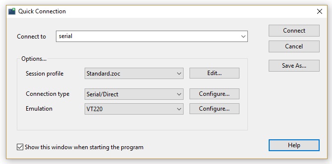
We also must install a terminal emulator application on the PC. A good choice is the EmTec ZOC emulator found here. It provides a wide range of terminal emulations and options as well as the capability of sending and receiving binary and text files. The latter will be useful later when we explore AVR Tiny BASIC.
Once installed, start ZOC and click File-Quick Connection. Configure ZOC as a VT220 terminal as shown below. Make sure that the Redboard USB is connected to the PC. Use "Scan..." to find the USB port in use by the Redboard. If more than one port shows, try all until the correct one is found. Click on "Configure" next to "Serial/Direct" and complete the option selection.
Click "Save As..." to create a desktop icon that makes future terminal startup quick and easy with a single click. We are ready to test serial I/O in Experiment 5 Example 1 below.
Experiment 10-5 Basic iterative Structures - The WAIT-DO LOOP with the ATmega328
Recall the flow chart for the WAIT-DO LOOP.
| WAIT-DO LOOP |
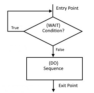 |
We use the WAIT-DO LOOP to poll the USART to determine if it has keyboard data ready to input or if it's busy outputting a previously received character. WAIT-DO coding with the ATmega328 follows the Intel 8080 very closely.
Try it!
Experiment 10-5 Example 1. Code a terminal input/output (echo) routine.
The ATmega328 code below is essentially the same as the Intel 8080. Note that the ATmega329 STS and LDS instructions are used instead of OUT and IN for the reason given in the "Note" above. Consult section 24.12 of the ATmega328 Datasheet for a description of I/O registers such as "ucsr0a".
;
; Experiment 5 Example 1a Terminal Echo Code using mask and ANDI
;
exmp5_1a:
;
chrina:
lds
r17, ucsr0a
;get USART receive status byte
andi r17,
0b10000000 ;mask bit 7 (RXC0=7) of UCSR0A (USART receive
complete), a one indicating character available (Search "Bit 7 – RXC0")
breq chrina
;loop and wait
lds
r16, udr0
;otherwise, get character into r16
;
chrouta:
lds
r17, ucsr0a
;get USART transmit status byte
andi r17,
0b00100000 ;mask bit 5 (UDRE0=5) of UCSR0A (USART
transmit buffer empty), a one indicating transmit buffer empty (Search "Bit 5 –
UDRE0")
breq chrouta
;loop and wait
sts
udr0, r16
;otherwise, output character in r16
;
rjmp chrina
;repeat
;
Change the Target Jump line to "exmp5_1a". Build the solution and program the ATmega328 flash memory to test the program. With the terminal program operating, characters typed on the keyboard should echo on the screen.
In the code below we have rewritten the echo routine to take advantage of the ATmega328's "skip next instruction" instructions below.
| ATmega328 Instruction |
Comment |
| SBIC A,b | Skip next instruction if bit b in I/O register A is cleared |
| SBIS A,b | Skip next instruction if bit b in I/O register A is set |
| SBRC Rr,b | Skip next instruction if bit b in working register Rr is cleared |
| SBRS Rr,b | Skip next instruction if bit b in working register Rr is set |
In both the serial input and serial output routines, the loop jump instruction is skipped when the receive or transmit status shows ready. The skip instructions allow us to directly test the bit by number (e.g.,RCX0 =7 and UDRE0=5). Here is the echo code using skip instructions instead of masking with an AND instruction.
;
; Experiment 5 Example 1b Terminal Echo Code using ATmega328 bit-wise testing
;
exmp5_1b:
;
chrinb:
lds
r17, ucsr0a
;get USART receive status byte
sbrs r17,
rxc0
;skip next instruction if bit 7 (RXC0=7) of UCSR0A (USART receive complete) is
one indicating character available (Search "Bit 7 – RXC0")
rjmp chrinb
;loop and wait (instruction skipped if character available)
lds
r16, udr0
;get character into r16
;
chroutb:
lds
r17, ucsr0a
;get USART transmit status byte
sbrs r17,udre0
;skip next instruction if bit 5 (UDRE0=5) of UCSR0A (USART transmit buffer
empty) is one indicating transmit buffer empty (Search "Bit 5 – UDRE0")
rjmp chroutb
;loop and wait (instruction skipped if not busy outputting character)
sts
udr0, r16
;output character in r16
;
rjmp chrinb
;repeat
;
Change the Target Jump line to "exmp5_1b". Build the solution and program the ATmega328 flash memory to test the program. With the terminal program operating, characters typed on the keyboard should echo on the screen.
Note: Skip I/O instructions work only with registers above the 0 to 31 range . Unfortunately, USART I/O registers like "ucsr0a" are much higher (192), so we have to use the LDS instruction to first load them into a working register and then use the register skip instruction.
To take full advantage of our serial communication capability, we add the following utility subroutines to Experiment_10's main.asm:
| Subroutine Name | Description |
| chrin | Returns a character from the keyboard in register r16 |
| chrout | Displays the character in register r16 on the PC screen |
| msgout | Displays the character message pointed to by register z (sentinel value is zero byte) |
| binout | Displays the 8-bit value in register r16 in binary format |
| hexout | Displays the 8-bit value in register r16 in hex format |
| decout | Displays the 8-bit value in register r16 in decimal format |
| crlf | Displays a new line (carriage return and line feed) |
| delay | Delays approximate 2 seconds |
| delay_ms | Delays for milliseconds specified in x register |
| delay_10ms | Delays for 10 milliseconds |
| delay_1s | Delays for 1 second |
| delay_2s | Delays for 2 seconds |
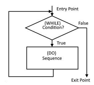
Experiment 10-5 Basic iterative Structures - The WHILE-DO LOOP
The basic WHILE-DO loop looks like this.
Try it!
Experiment 10-5 Example 2 Sum the consecutive integers from 0 to N where N is equal to or greater than zero. No great surprises here. The ATmega328 code conversion is generally one-to-one with register r16 chosen as accumulator.
The subroutine "decout" is used to display the result in r16 as ASCII. It uses the used defined "T" flag to pass information from the calling routine. Setting the "T" flag before calling "decout" inhibits leading zeros. If "T" is cleard, the displayed answer for N=5 would be "015". The call to "crlf" moves the screen cursor to a new line by displaying, in succession, an ASCII carriage return and linefeed. After execution, the code enters an endless loop at "halt". To repeat execution, press and release the "RESET" button on the Redboard (located near the usb cable jack).
With the Intel 8080, we had to accumulate the sum and test the counter in the A register thus requiring several extra bytes of code. Since all ATmege328 registers can act as accumulators, we can separate the functions into two registers saving a few bytes of code. See the area highlighted in yellow below.
;
; Experiment 5 Example 2a Sum Integers Using DO-WHILE (with error trap)
;
; Sum integers from 0 to sum limit and display result
;
; Also, test 22 then 23. The latter should produce an error.
;
exmp5_2a:
call crlf
;display new line
ldi
r18,5
;set sum limit (test value = 5 Result = 0 + 1 + ... + 5 = 15)
clr
r16
;clear sum
clr
r2
;clear counter
exmp5_2a_again:
cp
r18,r2
;does counter equal sum limit?
breq exmp5_2a_done
;if, branch to done
inc r2
;increment counter
add r16,r2
;add counter to sum
brcs exmp5_2a_error
;if overflow, trap error
rjmp
exmp5_2a_again
;otherwise, do again
;
exmp5_2a_done:
set
;inhibit leading zeros
call decout
;display decimal value
jmp halt
;jump to endless loop
;
; Error Trap
;
exmp5_2a_error:
ldi
r16,'E'
;display letter E for error
call chrout
jmp halt
;branch to endless loop
;
;
; Endless Loop
;
halt:
rjmp halt
;jump to self
Change the Target Jump line to "exmp5_2a". Build the solution and program the ATmega328 flash memory to test the program. With the sum limit set to "5", the sum "15" should display. Try different values for the sum limit including "23" that should produce an error.
Notice that we ended up with adjacent branch and jump (highlighted in green above). Whenever adjacent jumps or branches arise while coding, we can recode to eliminate one of the them. In this case, we notice that by by moving the "error" code up and changing the branch from "carry clear" to "carry set", the relative jump can be eliminated. See the code highlighted in blue below.
;
; Experiment 5 Example 2b Sum Integers Using DO-WHILE (with error trap)
;
; Elimination of consecutive branches
;
; Sum integers from 0 to sum limit and display result
;
; Also, test 22 then 23. The latter should produce an error.
;
exmp5_2b:
call crlf
;display new line
ldi
r18,5
;set sum limit
clr
r16
;clear sum
clr
r2
;clear counter
exmp5_2b_again:
cp
r18,r2
;does counter equals sum limit?
breq exmp5_2b_done
;if so, branch to done
inc r2
;increment counter
add r16,r2
;add counter to sum
brcc exmp5_2b_again
;if no overflow, do again
;
; Error Trap
;
ldi
r16,'E'
;display letter E for error
call chrout
jmp halt
;branch to endless loop
;
exmp5_2b_done:
set
;inhibit leading zeros
call decout
;display decimal value
jmp halt
;jump to endless loop
Change the Target Jump line to "exmp5_2b". Build the solution and program the ATmega328 flash memory to test the program.
Finally, recall that we simplified the Intel 8080 program still more by rewriting code to decrement and accumulate the sum limit itself. Below is that version converted to ATmega328.
;
; Experiment 5 Example 2c Sum Integers Using DO-WHILE (with error trap)
;
; Elimination of consecutive branches AND separate counter
;
; Sum integers from 0 to sum limit and display result
;
; Test 22 then 23. The latter should produce an error.
;
exmp5_2c:
call crlf
;display new line
ldi
r18,5
;set sum limit/counter
inc r18
;pre-increment sum limit/counter
clr r16
;clear sum
exmp5_2c_again:
dec r18
;does combined sum limit/counter equal zero?
breq exmp5_2c_done
;if so, branch to done
add r16,r18
;add sum limit/counter to sum
brcc exmp5_2c_again
;if no overflow, do again
;
; Error Trap
;
ldi
r16,'E'
;display letter E for error
call chrout
jmp halt
;branch to endless loop
;
exmp5_2c_done:
set
;inhibit leading zeros
call decout
;display decimal value
jmp halt
;jump to endless loop
Change the Target Jump line to "exmp5_2c". Build the solution and program the ATmega328 flash memory to test the program.
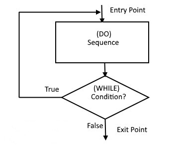
Experiment 10-5 Basic iterative Structures - DO_WHILE LOOP
The basic DO-WHILE loop looks like this.
Try it!
Experiment 10-5 Example 3 Using binary display on the PC screen, make a right-to-left chasing bit.
Example three uses the bit shift operators. The shift through carry operators for the Intel 8080 (RAL and RAR) and ATmega328 (ROL and ROR) are identical except that the latter can operate on any working register.
The "not through carry" shift operators, however, are slightly different. The Intel 8080 and ATmega328 versions are alike in that they shift the most or least significant bit into carry depending on right or left shift respectively. Where they differ is that the Intel 8080 shifts the least significant bit (bit 0) to the most significant bit (bit 7) for RRC and shifts the most significant bit (bit 7) to the least significant bit (bit 0) for RLC. The ATmega328 instead shifts a zero into the most significant bit (bit 7) for LSR and shifts a zero into the least significant bit (bit 0) for LSL. The ATmega328's handling of this shift seems more logical when interpreting the shift operation as multiplying or dividing by two. For example, the Intel 8080 RLC instruction operating on 0b10000001 (128 decimal) produces 0b00000011 (3 decimal) and carry set. This would indicate that 2 x 128 is 256 + 3 = 259 that is incorrect. The same code with the ATmega328 produces the correct result, 256+ 2 = 258!
The ATmega328 conversion below follows closely the Intel 8080 code. Binary display "binout" and delay "delay" subroutines are used. The former displays the value of r16 in binary 1s and 0s as they rotate while the latter introduces a time delay between binary displays of about two seconds.
Both versions of the chasing bit code (right-to-left and left-to-right) are shown below.
;
; Experiment 5 Example 3a Chasing Bit Display - Right to Left
;
; Displayed one bit moves from right to left
;
exmp5_3a:
ldi
r20,0b00000001 ;load r20 with 1
in right most bit (bit 0)
exmp5_3a_again:
call
crlf
;display new line
mov r16,r20
;display r20
call
binout
call
delay
;wait 2 seconds
clc
;clear carry
rol
r20
;rotate r20 left through carry
brcc exmp5_3a_again
;until bit reaches carry, do again
rjmp exmp5_3a
;start over
;
; Experiment 5 Example 3b Chasing Bit Display - Left to Right
;
; Displayed one bit moves from left to right
;
exmp5_3b:
ldi
r20,0b10000000 ;load r20 with 1
in left most bit (bit 7)
exmp5_3b_again:
call
crlf
;display new line
call
delay
;wait 2 seconds
mov
r16,r20
;display r20
call
binout
clc ;clear carry
ror
r20
;rotate r20 right through carry
brcc
exmp5_3b_again ;until bit
reaches carry, do again
rjmp exmp5_3b
;start over
Change the Target Jump line to "exmp5_3a". Build each solution and program the ATmega328 flash memory to test the program. Repeat for "exmp_5_3b".
Experiment 10-5 Memory Access - Direct Memory Access
Recall that the Intel 8080 had two instructions that read and write directly to memory. These were LDA k and STA k where k can range over 0 to 65,535. Direct memory access instructions for the ATmega328 allow access to (1) the working registers, (2) the I/O registers, and (3) all of SRAM. The ATmega328 direct memory access instructions are LDS k and STS k where k can range from 0 to 2,303 (0x08FF). For reference, see the Data Memory Map for the ATmega328 below.
| IN/OUT Instruction | ATmega328 Memory | LDS/STS Instruction |
| r0 to r31 32 working Registers | 0x0000 to 0x001F | |
| 0x0000 to 0x003F | 64 I/O Registers | 0x0020 to 0x005F |
| 160 External I/O Registers | 0x0060 to 0x00FF | |
| SRAM | 0x0100 to 0x08FF |
The ATmega328 has no direct way to read or write directly to program memory though there is an indirect way to do so. See the next section.
Note: ATmega328's stack pointer is initialized to the end of SRAM and builds downward. Usually this is not a problem as PUSH's and POP's cancel each other over time. However, we must take care using upper regions of SRAM as it poses a possibility of creating a conflict. Recall also that SRAM is volatile memory and its contents disappear when power is off. Given these restrictions, data can be stored and recall from SRAM beginning at address 0x0100.
Try it!
Experiment 10-6 Example 1 Use SRAM as temporary storage for the data character in the echo program.
The ATmega328 assembler distinguishes between program memory and data memory using the mode directives .cseg (code segment) and .dseg (data segment). Unless changed by the .org directive, the code segment initializes at 0x0000 in program memory and the data segment initializes at 0x0100 in the SRAM. Code segment is the default mode at the start of assembly. Both with .cseg and .dseg, the assembler keeps separate track of the next address to be used in their respective memories.
In this example, we switch to the data segment and set aside a single byte labeled "char" to use as temporary storage for the typed keyboard character while waiting to display it. The physical address for "char" is 0x0100 since it is the first byte to be allocated in the data segment. Were we to reserve another byte, it would be at 0x0101. Switching back to the code segment, the next program instructions will continue at the program memory address following the last assembled instruction.
;
; Experiment 6 Example 1 Terminal Echo Code using mask, ANDI, and temporary
storage in SRAM
;
exmp6_1:
;
; Note: Since this is the first data segment (.dseg) byte reserved, it will get
the address 0x0100. The next
; reserved byte will get the address 0x0101 and so on. The assembler keeps up
with data bytes
; are reserved.
;
exmp6_1_chrina:
lds
r17, ucsr0a
;get USART receive status byte
andi r17,
(1<<rxc0)
;does rxc0 bit = 0
breq exmp6_1_chrina
;if so, loop and wait until input character available
lds
r16, udr0
;otherwise, get character into r16
sts
char,r16
;save character in SRAM
;
.dseg
;data segment (data memory)
;
char: .byte 1
;reserve 1 byte in SRAM
;
.cseg
;return to code segment (program memory)
;
exmp6_1_chrouta:
lds
r17, ucsr0a
;get USART transmit status byte
andi r17,
(1<<udre0) ;does udre0 bit = 0
breq
exmp6_1_chrouta ;if so, then loop and wait until
no longer busy outputting character
lds
r16,char
;get character from SRAM
sts
udr0, r16
;otherwise, output character in r16
;
rjmp exmp6_1_chrina
;start over
;
Experiment 10-6 Example 2 Sum two 16-bit values and store the result in SRAM.
The first thing to note is the macro "ldiw" load word immediate (highlighted in green). As mentioned, the Atmega328 is lacking in double byte instructions, but we can create macros to do the job. The reference to "load immediate word" macro looks like this "ldiw rh, rl, k". The high byte of the16-bit constant k loads into the first working register listed (rh) and the lower byte loads into rl. Common practice with the ATmega328 is to designate the first of a working register pair as the high byte and the second working register as the low byte. If the pair were r0 and r1, we would write in as r0 : r1 to emphasize it is a double byte value. To load the working register pair r0 : r1 with 10,000, we would use "ldiw r0, r1, 10000". For the x, y, and z register pairs, high and low bytes can be designated by adding a "h" or "l" suffix. For example, z is r30 : r31, but we can refer to them as "zh" for r30 and "zl" for r31. To load the z register with 10000, we could use either "ldiw r30, r31, 10000" or "ldiw zh, zl, 10000".
Since we don't have a double add instruction like the Intel 8080 "DAD", we use the combination of "add" and "adc" (highlighted in yellow). We could easily create an "addw" macro to perform double byte adds in the future.
Finally, we use the "STS" and "LDS" instructions to store and load the sum in consecutive bytes of memory (high lighted in blue). The 8-bit decimal display subroutine provides a way to check the result.
;
; Load Register Immediate Word Macro
;
.macro ldiw
ldi @0, high(@2)
ldi @1, low(@2) ;subtract the negative of an immediate value
.endmacro
;
; . . .
;
; Experiment 6 Example 2 Add two 16-bit values in program memory then store in
data memory (SRAM)
;
exmp6_2:
;
.equ first_num = 1000 ;first value to be added
.equ second_num = 250
;second value to be added
;
.dseg
;data segment (data memory)
;
sum: .byte 2 ;reserve
2 bytes in SRAM for sum result
;
.cseg
;return to code segment (program memory)
;
ldiw r16,r17,first_num ;load first number in r17:r16
;
ldiw r18,r19,second_num ;load second number in r19:r18
;
add r17,r19
;add r16:r17 and r18:r19
adc r16,r18
;
sts sum,r16 ;store in SRAM
sts sum+1,r17
;
call crlf ;display new line
lds r16,sum ;get most significant byte (msb) and display it as decimal
call decout
lds r16,sum+1 ;get least significant byte (lsb) and display it as decimal
call decout
;
; Note: Final result is msb * 256 + lsb. 4 *256 + 226 = 1250!
;
jmp halt
Change the Target Jump line to "exmp6_2". Build the solution and program the ATmega328 flash memory to test the program.
Experiment 10 Memory Access - Indirect Memory Access
The Intel 8080 has three working register pairs that provide indirect memory access to the 65,535 bytes of its memory. The register pairs are HL (the most versatile) , BC, and DE. The ATmega328 also has three working register pairs r31 : r30 (the z register pair and the most versatile), r26 : r27 (the x register pair), and r28 : r29 (the y register pair). The z register can access both program and data memory. The x and y registers access only the data memory. While the ATmega328 has no double byte operator capability like the Intel 8080's "m" register, it does have a greater variety of instructions to facilitate indirect addressing. The first table below summarizes data memory access instructions; the second table shows those that access program memory. Note that there is no instruction to store in program memory. This is a wise design restriction given the problems that can accrue from the self-altering programs.
Note: Of particular interest are the pre and post incrementing versions of the instructions. These are very useful when working with tables. See the examples below.
| Indirect Memory Access - Data Memory | ||
| ATmega328 Instruction | Description | Similar 8080 Instruction |
| LD Rd, x | Load indirect from address x register: (x) -> Rd | LDAX B, LDAX D, MOV A,M |
| LD Rd, x+ | Load indirect from address x register then increment x: (x) -> Rd then x + 1 -> x | |
| LD Rd, -x | Decrement x then load indirect from x register: x - 1 -> x then (x) -> Rd | |
| LD Rd, y | Load indirect from address y register: (y) -> Rd | LDAX B, LDAX D, MOV A,M |
| LD Rd, y+ | Load indirect from address y register then increment y: (y) -> Rd then y + 1 -> y | |
| LD Rd, -y | Decrement y then load indirect from y register: y - 1 -> y then (y) -> Rd | |
| LD Rd ,z | Load indirect from address z register: (z) -> Rd | LDAX B, LDAX D, MOV A,M |
| LD Rd, z+ | Load indirect from address z register then increment z: (z) -> Rd then z + 1 -> z | |
| LD Rd, -z | Decrement z then load indirect from z register: z - 1 -> z then (z) -> Rd | |
| LDD Rd, y+d | Load indirect from address y plus displacement d (0 ≥ d ≤ 31) | |
| LDD Rd, z+d | Store indirect from address z plus displacement d (0 ≥ d ≤ 31) | |
| ST Rd, x | Store indirect from address x register: (x) -> Rd | STAX B, STAX D, MOV M,A |
| ST Rd, x+ | Store indirect from address x register then increment x: (x) -> Rd then x + 1 -> x | |
| ST Rd, -x | Decrement x then store indirect from x register: x - 1 -> x then (x) -> Rd | |
| ST Rd, y | Store indirect from address y register: (y) -> Rd | STAX B, STAX D, MOV M,A |
| ST Rd, y+ | Store indirect from address y register then increment y: (y) -> Rd then y + 1 -> y | |
| ST Rd, -y | Decrement y then store indirect from y register: y - 1 -> y then (y) -> Rd | |
| ST Rd ,z | Store indirect from address z register: (z) -> Rd | STAX B, STAX D, MOV M,A |
| ST Rd, z+ | Store indirect from address z register then increment z: (z) -> Rd then z + 1 -> z | |
| ST Rd, -z | Decrement z then store indirect from z register: z - 1 -> z then (z) -> Rd | |
| STD Rd, y+d | Store indirect from address y plus displacement d (0 ≥ d ≤ 31) | |
| STD Rd, z+d | Store indirect from address z plus displacement d (0 ≥ d ≤ 31) | |
| Indirect Memory Access - Program Memory | ||
| ATmega328 Instruction | Description | Similar Intel 8080 Instruction |
| LPM | Load R0 indirect from z register: (z) -> R0 | MOV A,M |
| LPM Rd, z | Load Rd indirect from z register: (z) -> Rd | |
| LPM z+ | Load Rd indirect from z register then increment z: (z) -> Rd then x + 1 -> x | |
Try it!
Experiment 6 Example 3 Sum the list of single byte integers (3,12,32,14,13,38,0, and -5) and display the total on the PC screen.
A slight complication arises when we store a list of 8-bit byte values in the ATmega328's 16-bit program memory. The AVR designers could have simply wasted the extra 8 bits and stored only one 8-bit byte at each 16-bit program memory address. Instead they developed a clever way to store two 8-bit value at each 16-bit program memory address. The LPM instruction uses the zero bit of the z register to designate which half of the 16-bit byte is to be accessed. If z's bit 0 is zero, the lower 8-bit value is accessed; if z's bit 0 is a one, the upper byte is accessed. This means that when we load the z register with a particular address, we shift the actual address left one position knowing that the LPM instruction will handle bit 0. Thus, in the "ldiw z" instruction below highlighted in yellow, we use (d_tbl << 1) to shift the actual address once to the left. The LPM instruction later on takes this into account when loading the two bytes per word values stored in program memory. The assembler directive ".db" packs the values two bytes at each 16-bit program memory address. This leads to an annoying "feature" of the assembler. If we reserve an odd number of values in program memory, the assembler generates a warning message that the upper byte of the last memory address will be loaded with zeros. To avoid the message, always reserve an even number of bytes. That is, if the warning message appears, add a zero byte to the ".db" line. See the line below highlighted in green.
The list below shows how the data 3,12,32,14,13,38,0,-5 is stored after an assembly. Note that "3" is stored in the lower byte of the first program memory address. The next value, 12 (0x0C), is stored in the upper half and so forth. To access this data, we would load z with 0x00b8 shifted left once then rely on the LPM instruction to pick its way through the list while incrementing z.
0000b8 0C03
;3,12 (in reverse order; i.e., 3 in lower byte and 12 in upper byte)
0000b9 0E20 ;32,14
0000ba 260D ;13,38
0000bb FB00 ;0,-5
The 8 data bytes are stored in 4 program memory addresses wasting no space.
;
; Experiment 6 Example 3 Sum Signed Number from Program Memory List Using
DO-WHILE (with error trap)
;
; Sum integers in a list of know length and display result
;
exmp6_3:
call
crlf
;display new line
ldiw zh,zl,(d_tbl<<1)
;point z register to start of data table
clr
r16
;clear sum
ldi
r20,8
;load count
exmp6_3_again:
lpm
;load byte into r0 (r0 implied for lpm)
add r16,r0
;add byte to sum
brvs exmp6_3_error
;if signed number overflow, trap error
adiw zh:zl,1
;point next byte
dec r20
;added all bytes?
brne exmp6_3_again
;if not, do again
call decout
;otherwise, display decimal value
jmp halt
;jump to endless loop
;
; Error Trap
;
exmp6_3_error:
ldi
r16,'E'
;display letter E for error
call chrout
jmp halt
;branch to endless loop
;
d_tbl: .db 3,12,32,14,13,38,0,-5 ;no error: result 107 in range -128 to +127
;
;d_tbl: .db 10,-120,-32,0 ;error; result less than -128 and out of range
Change the Target Jump line to "exmp6_3". Build the solution and program the ATmega328 flash memory to test the program.
Note: We took advantage of the ATmega328's signed number overflow flag (v flag) to trap a possible addition error. The "v flag" eliminates the rather confusing Intel 8080 code to trap such errors. To test for overflow, try the second set of data. Be sure to change the "load count" line (high lighted in blue) to "3" instead of "8".
Experiment 10-6 Example 4 Sum the list of single byte integers (3,12,32,14,13,38,0, and -5) and display the total on the PC screen. Assume the number of integers is not fixed and there are fewer than 256.
The program below follows the Intel 8080 example and the ATmega328 Example 3 above. There are three minor items to mention. First, the number of bytes calculated in r20 is doubled as the data is packed two bytes per 16-bit memory address. See the left shift LSL instruction highlighted in yellow. Next, the "lpm" instruction (highlighted in green) has been replaced by "lpm r0, z+". While doing indirect memory access, the pointer register (z in this case) is automatically incremented as the data is retrieved. Choosing the "z+" option eliminates the "add immediate word" instruction in Example 3 above. Finally, notice that the table end (d_tbl_e) data byte directive reserves two zeros (highlighted in blue). The second zero is there to avoid an assembler warning message.
;
; Experiment 6 Example 4 Sum Signed Number from Program Memory List Using
DO-WHILE (with error trap)
;
; Sum integers in a list of unknown length and display result
;
exmp6_4:
ldi
r20, low(d_tbl_e) ;calculate
number of bytes to add (assume < 256)
subi
r20, low(d_tbl_b)
lsl
r20
call
crlf
;display new line
ldiw zh,zl,(d_tbl_b<<1)
;point z register to start of data table
clr
r16
;clear sum
exmp6_4_again:
lpm r0,
z+
;load byte into r0 and increment z
add
r16,r0
;add byte to sum
brvs exmp6_4_error
;if signed number overflow, trap error
dec r20
;added all bytes?
brne exmp6_4_again
;if not, do again
call
decout
;otherwise, display decimal value
jmp halt
;jump to endless loop
;
; Error Trap
;
exmp6_4_error:
ldi
r16,'E'
;display letter E for error
call chrout
jmp halt
;branch to endless loop
;
d_tbl_b: .db 3,12,32,14,13,38,0,-5 ;no error
d_tbl_e: .db 0,0
Change the Target Jump line to "exmp6_4". Build the solution and program the ATmega328 flash memory to test the program.
Experiment 10-6 Example 5 With the message "Hello World" in program memory, display it to the PC screen.
The translation from Intel 8080 to ATmega328 is straightforward. The z register pair simply replaces HL in the original code. Note that the sentinel value zero to mark the end of the message is the twelfth byte and even. No padding byte is needed.
;
; Experiment 6 Example 5 Display the message "Hello World" Using WHILE-DO
;
; Display the ASCII text in program memory. Use numeric zereo as sentinel value.
;
exmp6_5:
call crlf
;display new line
ldiw zh,zl,(exmp6_5_msg<<1)
;point z register to start of message
exmp6_5_again:
lpm r16,z+
;load character into r16 and post increment z
or
r16,r16
;sentinel character reached?
breq exmp6_5_done
;if so, branch to halt
call chrout
rjmp exmp6_5_again
;do again
;
exmp6_5_done:
jmp halt
;jump to endless loop
;
exmp6_5_msg: .db "Hello World",0
Because displaying a message from program memory is so useful, we have included it as a utility routine. To access it, point the z register to the start of the message (remembering to shift left) and then call "msgout".
Change the Target Jump line to "exmp6_5". Build the solution and program the ATmega328 flash memory to test the program.
Experiment 6 Example 6 Convert a message to upper case and store it at a new address in memory. Display both messages on the PC screen to verify that the program worked correctly.
The original message is in program memory and the z register is used to load each message byte into register r16. The byte is translated to upper case if needed then written to the new address in data memory. As before, program memory is accessed using the "lpm r16,z+" instruction. The "st x+,r16" instruction stores the translated byte to data memory. Notice that the post increment option is used in both cases to move the pointers through the message. After translation is completed, the original message is displayed on the PC screen using the utility subroutine "msgout". To output the message in data memory, the z register is used as a pointer into data memory and the "ld r16,z+" instruction loads the message bytes into r16 for outputting with the "chrout" utility subroutine. In both instances, the zero byte is the sentinel value to mark message end.
;
; Experiment 6 Example 6 Convert Message to Upper Case Using WHILE-DO
;
; Display the original message and converted message
;
; Note: Test message limited to 50 characters
;
exmp6_6:
ldiw
zh,zl,(exmp6_6_msg<<1)
;point z register to original message
ldiw
xh,xl,(exmp6_6_ucmsg<<1) ;point
x register to space in SRAM
exmp6_6_loop0:
lpm
r16,z+
;load character into r16 and post increment z
or
r16,r16
;was sentinel character reached?
breq
exmp6_6_cont1
;if so, branch to continue 1
cpi
r16,'a'
;is character < 'a'?
brcs
exmp6_6_cont0
;if so, branch to continue 0
cpi
r16,'z'+1
;is character >= 'z'+1
brcc
exmp6_6_cont0
;if so, branch to continue 0
andi
r16,0b11011111
;make upper case
exmp6_6_cont0:
st
x+,r16
;store in SRAM
rjmp
exmp6_6_loop0
;do again
exmp6_6_cont1:
st
x,r16
;store sentinel value
;
; Display original message
;
call
crlf
;display new line
ldiw
zh,zl,(exmp6_6_msg<<1)
;point z register to start of message
call
msgout
;display original message
;
; Display translated message
;
call
crlf
;display new line
ldiw
zh,zl,(exmp6_6_ucmsg<<1)
;point z register to converted messagr in SRAM
exmp6_6_loop1:
ld
r16,z+
;load character into r16 and post increment z
or
r16,r16
;was sentinel character reached?
breq
exmp6_6_done
;if so, branch to halt
call
chrout
;display character
rjmp
exmp6_6_loop1
;do again
;
exmp6_6_done:
jmp
halt
;jump to endless loop
;
exmp6_6_msg: .db "Upper case test program: AB...Z = ab...z",'a'-1,'z'+1,0,0
;
.dseg
exmp6_6_ucmsg: .byte 50;
.cseg
;
Change the Target Jump line to "exmp6_6". Build the solution and program the ATmega328 flash memory to test the program.
Experiment 10-6 Example 7 Display a numeric value from a list based on a keyboard entry of digits 0 to 9.
Besides accepting data from the keyboard and displaying it on the PC screen, the only significant difference is that the ATmega328 lacks an add immediate with carry. To get around this, we clear register r16 and use the add register with carry, "adc zh,r16" (highlighted in yellow).
;
; Display a numeric value from a table based on keyboard entry of numbers 0 to
9.
;
; Note: Table length limited to 10 items.
;
exmp6_7:
ldiw zh,zl,(exmp6_7_tbl<<1)
;point z register to first entry in table
call
crlf
;display new line
call
chrin
;get character into r16
cpi
r16,'0'
;is character less than ASCII zero?
brcs
exmp6_7_error
;if so, branch to error
cpi
r16,'9'+1
;greater than ASCII nine plus 1
brcc
exmp6_7_error
;if so, branch to error
andi r16,0x0f
;mask off upper nibble to get table offset
add
zl,r16
;calculate low byte of table plus offset
clr
r16
;clear r16
adc
zh,r16
;calculate high byte of table entry address
lpm
r16,z
;load character into r16
set
;inhibit leading zeros
call
decout
rjmp
exmp6_7
;do again
;
;
; Error Trap
;
exmp6_7_error:
ldi
r16,'E'
;display letter E for error
call
chrout
jmp
exmp6_7
;do again
;
exmp6_7_tbl: .db 0,12,23,35,44,55,68,77,86,102
;
Change the Target Jump line to "exmp6_7". Build the solution and program the ATmega328 flash memory to test the program.
Experiment 10-6 Example 8 Input a single digit (0-9) from the keyboard then translate it into the equivalent word as shown in the table below and display it on the PC screen.
The translation is again straightforward and similar to Example 7. Note that in creating the pointer table (exmp_6_8_tbl_p) that the addresses of the word equivalents are rotated to the left anticipating they will be used later with a "lpm" instruction (highlighted in yellow).
;
; Experiment 6 Example 8 Demonstrate Table Look-Up Using Indirect Addressing -
Part 2
;
; Display the word representing keyboard entry of numbers 0 to 9.
;
; Note: Table length limited to 10 items.
;
exmp6_8:
ldiw
zh,zl,(exmp6_8_tbl_p<<1)
;point z register to first entry in table
call
crlf
;display new line
call
chrin
;get character into r16
cpi
r16,'0'
;is character less than ASCII zero?
brcs
exmp6_8_error
;if so, branch to error
cpi
r16,'9'+1
;is character greater than ASCII nine plus 1
brcc
exmp6_8_error
;if so, branch to error
andi r16,0x0f
;mask off upper nibble to get table offset
lsl
r16
;quadruple table offset (recall that addresses are times 2 and double byte)
lsl
r16
add zl,r16
calculate low byte of table entry address
clr
r16
;clear r16
adc zh,r16
;calculate high byte of table entry address
lpm r16,z+
;get address of first character in message
lpm zh,z
mov zl,r16
lpm r16,z
;load first character of message into r16
set
;inhibit leading zeros
call msgout
;display message
rjmp exmp6_8
;do again
;
;
; Error Trap
;
exmp6_8_error:
ldi
r16,'E'
;display letter E for error
call chrout
jmp exmp6_8
;do again
;
exmp6_8_tbl_p: .dd
(word_0<<1),(word_1<<1),(word_2<<1),(word_3<<1),(word_4<<1),(word_5<<1),(word_6<<1),(word_7<<1),(word_8<<1),(word_9<<1)
;
word_0: .db "Zero",0,0
word_1: .db "One",0
word_2: .db "Two",0
word_3: .db "Three",0
word_4: .db "Four",0,0
word_5: .db "Five",0,0
word_6: .db "Six",0
word_7: .db "Seven",0
word_8: .db "Eight",0
word_9: .db "Nine",0,0
Change the Target Jump line to "exmp6_8". Build the solution and program the ATmega328 flash memory to test the program.
This completes the comparison of Intel 8080 and ATmege328 coding. By now it should be clear that the major hurdle was recognizing the different set of mnemonics introduced with the ATmega328. Most of the program conversion was simply accomplished by replacing Intel 8080 mnemonics with ATmege328 mnemonics. Basic operation of both microprocessors was nearly the same. Learn it once and we can easily apply it again and again!
Continue to next Experiment - Click Here